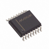
MAX187BCWE+ Maxim Integrated Products, MAX187BCWE+ Datasheet - Page 10

MAX187BCWE+
Manufacturer Part Number
MAX187BCWE+
Description
IC ADC SRL12BIT 5V 75KSPS 16SOIC
Manufacturer
Maxim Integrated Products
Datasheet
1.MAX189CCPA.pdf
(20 pages)
Specifications of MAX187BCWE+
Number Of Bits
12
Sampling Rate (per Second)
75k
Data Interface
MICROWIRE™, QSPI™, Serial, SPI™
Number Of Converters
1
Power Dissipation (max)
478mW
Voltage Supply Source
Single Supply
Operating Temperature
0°C ~ 70°C
Mounting Type
Surface Mount
Package / Case
16-SOIC (0.300", 7.50mm Width)
Number Of Adc Inputs
1
Architecture
SAR
Conversion Rate
75 KSPs
Resolution
12 bit
Input Type
Voltage
Interface Type
Serial
Voltage Reference
Internal 4.096 V
Supply Voltage (max)
5 V
Maximum Power Dissipation
478 mW
Maximum Operating Temperature
+ 70 C
Mounting Style
SMD/SMT
Minimum Operating Temperature
0 C
Lead Free Status / RoHS Status
Lead free / RoHS Compliant
+5V, Low-Power, 12-Bit Serial ADCs
The ADCs’ input tracking circuitry has a 4.5MHz small-
signal bandwidth, and an 8V/µs slew rate. It is possible
to digitize high-speed transient events and measure
periodic signals with bandwidths exceeding the ADC's
sampling rate by using undersampling techniques. To
avoid aliasing of unwanted high-frequency signals into
the frequency band of interest, an anti-alias filter is rec-
ommended. See the MAX274/MAX275 continuous-time
filters data sheet.
Internal protection diodes that clamp the analog input
allow the input to swing from GND - 0.3V to V
without damage. However, for accurate conversions
near full scale, the input must not exceed V
than 50mV, or be lower than GND by 50mV.
If the analog input exceeds the supplies by more than
50mV beyond the supplies, limit the input current to
2mA, since larger currents degrade conversion
accuracy.
The input lines to AIN and GND should be kept as short
as possible to minimize noise pickup. Shield longer
leads. Also see the Input Protection section .
Because the MAX187/MAX189 incorporate a T/H, the
drive requirements of the op amp driving AIN are less
stringent than those for a successive-approximation
ADC without a T/H. The typical input capacitance is
16pF. The amplifier bandwidth should be sufficient to
handle the frequency of the input signal. The MAX400
and OP07 work well at lower frequencies. For higher-
frequency operation, the MAX427 and OP27 are practi-
cal choices. The allowed input frequency range is limit-
10
Figure 5. MAX187/MAX189 Shutdown Sequence
______________________________________________________________________________________
SHDN
DOUT
CS
Driving the Analog Input
POWERED UP
CONVERSION 0
Input Bandwidth
Input Protection
DD
COMPLETE CONVERSION SEQUENCE
DD
by more
+ 0.3V
POWERED DOWN
ed by the 75ksps sample rate of the MAX187/MAX189.
Therefore, the maximum sinusoidal input frequency
allowed is 37.5kHz. Higher-frequency signals cause
aliasing problems unless undersampling techniques
are used.
The MAX187 can be used with an internal or external ref-
erence, while the MAX189 requires an external reference.
The MAX187 has an on-chip reference with a buffered
temperature-compensated bandgap diode, laser-
trimmed to +4.096V ±0.5%. Its output is connected to
REF and also drives the internal DAC. The output can
be used as a reference voltage source for other com-
ponents and can source up to 0.6mA. Decouple REF
with a 4.7µF capacitor. The internal reference is
enabled by pulling the SHDN pin high. Letting SHDN
float disables the internal reference, which allows the
use of an external reference, as described in the
External Reference section.
The MAX189 operates with an external reference at the
REF pin. To use the MAX187 with an external reference,
disable the internal reference by letting SHDN float. Stay
within the voltage range +2.5V to V
fied accuracy. The minimum input impedance is 12kΩ
for DC currents. During conversion, the external refer-
ence must be able to deliver up to 350µA DC load cur-
rent and have an output impedance of 10Ω or less. The
recommended minimum value for the bypass capacitor
is 0.1µF. If the reference has higher output impedance
or is noisy, bypass it close to the REF pin with a 4.7µF
capacitor.
t
WAKE
POWERED UP
CONVERSION 1
DD
External Reference
Internal Reference
to achieve speci-
Reference


