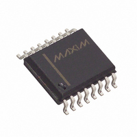
MAX187BCWE+ Maxim Integrated Products, MAX187BCWE+ Datasheet - Page 13

MAX187BCWE+
Manufacturer Part Number
MAX187BCWE+
Description
IC ADC SRL12BIT 5V 75KSPS 16SOIC
Manufacturer
Maxim Integrated Products
Datasheet
1.MAX189CCPA.pdf
(20 pages)
Specifications of MAX187BCWE+
Number Of Bits
12
Sampling Rate (per Second)
75k
Data Interface
MICROWIRE™, QSPI™, Serial, SPI™
Number Of Converters
1
Power Dissipation (max)
478mW
Voltage Supply Source
Single Supply
Operating Temperature
0°C ~ 70°C
Mounting Type
Surface Mount
Package / Case
16-SOIC (0.300", 7.50mm Width)
Number Of Adc Inputs
1
Architecture
SAR
Conversion Rate
75 KSPs
Resolution
12 bit
Input Type
Voltage
Interface Type
Serial
Voltage Reference
Internal 4.096 V
Supply Voltage (max)
5 V
Maximum Power Dissipation
478 mW
Maximum Operating Temperature
+ 70 C
Mounting Style
SMD/SMT
Minimum Operating Temperature
0 C
Lead Free Status / RoHS Status
Lead free / RoHS Compliant
Figure 10. MAX187/MAX189 Unipolar Transfer Function,
4.096V = Full Scale
Minimum cycle time is accomplished by using DOUT’s
rising edge as the EOC signal. Clock out the data with
13 clock cycles at full speed. Raise CS after the conver-
sion’s LSB has been read. After the specified minimum
time, t
next conversion.
The data output from the MAX187/MAX189 is binary,
and Figure 10 depicts the nominal transfer function.
Code transitions occur halfway between successive
integer LSB values. If V
1 LSB = 1.00mV or 4.096V/4096.
High-speed sampling capability and a 75ksps through-
put make the MAX187/MAX189 ideal for wideband sig-
nal processing. To support these and other related
applications, Fast Fourier Transform (FFT) test tech-
niques are used to guarantee the ADC’s dynamic fre-
quency response, distortion, and noise at the rated
throughput. Specifically, this involves applying a low-
distortion sine wave to the ADC input and recording the
digital conversion results for a specified time. The data
is then analyzed using an FFT algorithm that deter-
mines its spectral content. Conversion errors are then
seen as spectral elements outside of the fundamental
_____________Dynamic Performance
11 111
11 110
11 101
00 011
00 010
00 001
00 000
ACQ
OUTPUT CODE
Output Coding and Transfer Function
, CS can be pulled low again to initiate the
0
1
INPUT VOLTAGE (LSBs)
2
______________________________________________________________________________________
3
FULL-SCALE
TRANSITION
+5V, Low-Power, 12-Bit Serial ADCs
REF
= +4.096V, then
FS - 3/2LSB
FS = +4.096V
1LSB =
FS
4096
FS
input frequency. ADCs have traditionally been evaluat-
ed by specifications such as Zero and Full-Scale Error,
Integral Nonlinearity (INL), and Differential Nonlinearity
(DNL). Such parameters are widely accepted for speci-
fying performance with DC and slowly varying signals,
but are less useful in signal-processing applications,
where the ADC’s impact on the system transfer function
is the main concern. The significance of various DC
errors does not translate well to the dynamic case, so
different tests are required.
Signal-to-noise plus distortion (SINAD) is the ratio of the
fundamental input frequency’s RMS amplitude to the
RMS amplitude of all other ADC output signals. The
input bandwidth is limited to frequencies above DC and
below one-half the ADC sample (conversion) rate.
The theoretical minimum ADC noise is caused by quan-
tization error and is a direct result of the ADC’s resolu-
tion: SINAD = (6.02N + 1.76)dB, where N is the number
of bits of resolution. An ideal 12-bit ADC can, therefore,
do no better than 74dB. An FFT plot of the output
shows the output level in various spectral bands. Figure
11 shows the result of sampling a pure 10kHz sine
wave at a 75ksps rate with the MAX187/MAX189.
Figure 11. MAX187/MAX189 FFT plot
-100
-120
-140
-20
-40
-60
-80
20
0
0
FREQUENCY (kHz)
Signal-to-Noise Ratio and
Effective Number of Bits
18.75
f
f
T
S
T
A
= 75ksps
= 10kHz
= +25°C
37.5
13


