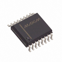
MAX187BCWE+ Maxim Integrated Products, MAX187BCWE+ Datasheet - Page 15

MAX187BCWE+
Manufacturer Part Number
MAX187BCWE+
Description
IC ADC SRL12BIT 5V 75KSPS 16SOIC
Manufacturer
Maxim Integrated Products
Datasheet
1.MAX189CCPA.pdf
(20 pages)
Specifications of MAX187BCWE+
Number Of Bits
12
Sampling Rate (per Second)
75k
Data Interface
MICROWIRE™, QSPI™, Serial, SPI™
Number Of Converters
1
Power Dissipation (max)
478mW
Voltage Supply Source
Single Supply
Operating Temperature
0°C ~ 70°C
Mounting Type
Surface Mount
Package / Case
16-SOIC (0.300", 7.50mm Width)
Number Of Adc Inputs
1
Architecture
SAR
Conversion Rate
75 KSPs
Resolution
12 bit
Input Type
Voltage
Interface Type
Serial
Voltage Reference
Internal 4.096 V
Supply Voltage (max)
5 V
Maximum Power Dissipation
478 mW
Maximum Operating Temperature
+ 70 C
Mounting Style
SMD/SMT
Minimum Operating Temperature
0 C
Lead Free Status / RoHS Status
Lead free / RoHS Compliant
The MAX187/MAX189 serial interface is fully compatible
with SPI, QSPI, and Microwire standard serial
interfaces.
If a serial interface is available, set the CPU’s serial
interface in master mode so the CPU generates the ser-
ial clock. Choose a clock frequency up to 2.5MHz.
1. Use a general-purpose I/O line on the CPU to pull CS
2. Wait the for the maximum conversion time specified
3. Activate SCLK for a minimum of 13 clock cycles. The
Figure 14. SPI/Microwire Serial Interface Timing (CPOL = CPHA = 0)
Figure 15. QSPI Serial Interface Timing (CPOL = CPHA = 0)
____________Applications Information
low. Keep SCLK low.
before activating SCLK. Alternatively, look for a
DOUT rising edge to determine the end of
conversion.
first falling clock edge will produce the MSB of the
DOUT conversion. DOUT output data transitions on
DOUT
SCLK
HI-Z
CS
Connection to Standard Interfaces
t CONV
EOC
DOUT
SCLK
HI-Z
______________________________________________________________________________________
CS
t CONV
MSB
+5V, Low-Power, 12-Bit Serial ADCs
D10
EOC
1ST BYTE READ
D9
D8
MSB
D7
D10
D6
D9
D5
D8
D7
4. Pull CS high at or after the 13th falling clock edge. If
5. With CS = high, wait the minimum specified time, t
Data can be output in 1-byte chunks or continuously, as
shown in Figure 8. The bytes will contain the result of
the conversion padded with one leading 1, and trailing
0s if SCLK is still active with CS kept low.
D6
SCLK’s falling edge and is available in MSB-first for-
mat. Observe the SCLK to DOUT valid timing charac-
teristic. Data can be clocked into the µP on SCLK’s
rising edge.
CS remains low, trailing zeros are clocked out after
the LSB.
before launching a new conversion by pulling CS
low. If a conversion is aborted by pulling CS high
before the conversions end, wait for the minimum
acquisition time, t
conversion.
D4
D5
D4
D3
D3
D2
D2
2ND BYTE READ
ACQ
D1
D1
LSB
, before starting a new
LSB
HI-Z
HI-Z
CS
15
,


