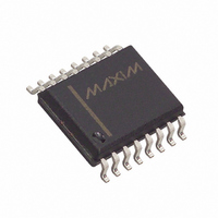
MAX187BCWE+ Maxim Integrated Products, MAX187BCWE+ Datasheet - Page 11

MAX187BCWE+
Manufacturer Part Number
MAX187BCWE+
Description
IC ADC SRL12BIT 5V 75KSPS 16SOIC
Manufacturer
Maxim Integrated Products
Datasheet
1.MAX189CCPA.pdf
(20 pages)
Specifications of MAX187BCWE+
Number Of Bits
12
Sampling Rate (per Second)
75k
Data Interface
MICROWIRE™, QSPI™, Serial, SPI™
Number Of Converters
1
Power Dissipation (max)
478mW
Voltage Supply Source
Single Supply
Operating Temperature
0°C ~ 70°C
Mounting Type
Surface Mount
Package / Case
16-SOIC (0.300", 7.50mm Width)
Number Of Adc Inputs
1
Architecture
SAR
Conversion Rate
75 KSPs
Resolution
12 bit
Input Type
Voltage
Interface Type
Serial
Voltage Reference
Internal 4.096 V
Supply Voltage (max)
5 V
Maximum Power Dissipation
478 mW
Maximum Operating Temperature
+ 70 C
Mounting Style
SMD/SMT
Minimum Operating Temperature
0 C
Lead Free Status / RoHS Status
Lead free / RoHS Compliant
Figure 6. Average Supply Current vs. Conversion Rate
When power is first applied, it takes the fully dis-
charged 4.7µF reference bypass capacitor up to 20ms
to provide adequate charge for specified accuracy.
With SHDN not pulled low, the MAX187/MAX189 are
now ready to convert.
To start a conversion, pull CS low. At CS’s falling edge,
the T/H enters its hold mode and a conversion is initiat-
ed. After an internally timed 8.5µs conversion period,
the end of conversion is signaled by DOUT pulling
high. Data can then be shifted out serially with the
external clock.
Power consumption can be reduced significantly by
shutting down the MAX187/MAX189 between conver-
sions. This is shown in Figure 6, a plot of average sup-
ply current vs. conversion rate. Because the MAX189
uses an external reference voltage (assumed to be pre-
sent continuously), it "wakes up" from shutdown more
quickly, and therefore provides lower average supply
currents. The wakeup-time, t
SHDN deasserted to the time when a conversion may
be initiated. For the MAX187, this time is 2µs. For the
MAX189, this time depends on the time in shutdown
(see Figure 7) because the external 4.7µF reference
bypass capacitor loses charge slowly during shutdown
(see the specifications for shutdown, REF Input Current
= 10µA max).
____________________Serial Interface
Using
10000
1000
100
10
1
0.1
Initialization After Power-Up and
SHDN
______________________________________________________________________________________
1
CONVERSIONS PER SECOND
to Reduce Supply Current
10
*REF CONNECTED TO V
Starting a Conversion
100
MAX187
+5V, Low-Power, 12-Bit Serial ADCs
WAKE,
1000
MAX189*
10000
is the time from
DD
100000
Figure 7. t
The actual conversion does not require the external
clock. This frees the µP from the burden of running the
SAR conversion clock, and allows the conversion result
to be read back at the µP’s convenience at any clock
rate from 0MHz to 5MHz. The clock duty cycle is unre-
stricted if each clock phase is at least 100ns. Do not
run the clock while a conversion is in progress.
Conversion-start and data-read operations are con-
trolled by the CS and SCLK digital inputs. The timing
diagrams of Figures 8 and 9 outline the operation of the
serial interface.
A CS falling edge initiates a conversion sequence: The
T/H stage holds input voltage, the ADC begins to con-
vert, and DOUT changes from high impedance to logic
low. SCLK must be kept inactive during the conversion.
An internal register stores the data when the conversion
is in progress.
End of conversion (EOC) is signaled by DOUT going
high. DOUT’s rising edge can be used as a framing
signal. SCLK shifts the data out of this register any time
after the conversion is complete. DOUT transitions on
SCLK’s falling edge. The next falling clock edge pro-
duces the MSB of the conversion at DOUT, followed by
the remaining bits. Since there are 12 data bits and one
leading high bit, at least 13 falling clock edges are
needed to shift out these bits. Extra clock pulses occur-
ring after the conversion result has been clocked out,
and prior to a rising edge of CS, produce trailing 0s at
DOUT and have no effect on converter operation.
3.0
2.5
2.0
1.5
1.0
0.5
WAKE
0
0.0001
vs. Time in Shutdown (MAX187 only)
0.001
TIME IN SHUTDOWN (sec)
0.01
0.1
Timing and Control
External Clock
1
10
11


