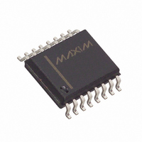
MAX187BCWE+ Maxim Integrated Products, MAX187BCWE+ Datasheet - Page 17

MAX187BCWE+
Manufacturer Part Number
MAX187BCWE+
Description
IC ADC SRL12BIT 5V 75KSPS 16SOIC
Manufacturer
Maxim Integrated Products
Datasheet
1.MAX189CCPA.pdf
(20 pages)
Specifications of MAX187BCWE+
Number Of Bits
12
Sampling Rate (per Second)
75k
Data Interface
MICROWIRE™, QSPI™, Serial, SPI™
Number Of Converters
1
Power Dissipation (max)
478mW
Voltage Supply Source
Single Supply
Operating Temperature
0°C ~ 70°C
Mounting Type
Surface Mount
Package / Case
16-SOIC (0.300", 7.50mm Width)
Number Of Adc Inputs
1
Architecture
SAR
Conversion Rate
75 KSPs
Resolution
12 bit
Input Type
Voltage
Interface Type
Serial
Voltage Reference
Internal 4.096 V
Supply Voltage (max)
5 V
Maximum Power Dissipation
478 mW
Maximum Operating Temperature
+ 70 C
Mounting Style
SMD/SMT
Minimum Operating Temperature
0 C
Lead Free Status / RoHS Status
Lead free / RoHS Compliant
The ADC results are transmitted across a 1500V isola-
tion barrier provided by three 6N136 opto-isolators.
Isolated power must be supplied to the converter and
the isolated side of the opto-couplers. 74HC595 three-
state shift registers are used to construct a 12-bit paral-
lel data output. The timing sequence is identical to the
timing shown in Figure 8. Conversion speed is limited
by the delay through the opto-isolators. With a 140kHz
clock, conversion time is 100µs.
The universal 12-bit parallel data output can also be
used without the isolation stage when a parallel inter-
face is required. Clock frequencies up to 2.9MHz are
possible without violating the 20ns shift-register setup
time. Delay or invert the clock signal to the shift regis-
ters beyond 2.9MHz.
For best performance, use printed circuit boards. Wire-
wrap boards are not recommended. Board layout
should ensure that digital and analog signal lines are
separated from each other. Do not run analog and digi-
tal (especially clock) lines parallel to one another, or
digital lines underneath the ADC package.
Figure 17 shows the recommended system ground
connections. A single-point analog ground (“star”
ground point) should be established at GND, separate
from the logic ground. All other analog grounds should
be connected to this ground. The 16-pin versions also
have a dedicated DGND pin available. Connect DGND
to this star ground point for further noise reduction. No
other digital system ground should be connected to
this single-point analog ground. The ground return to
the power supply for this ground should be low imped-
ance and as short as possible for noise-free operation.
High-frequency noise in the V
affect the ADC’s high-speed comparator. Bypass this
supply to the single-point analog ground with 0.01µF
and 4.7µF bypass capacitors. Minimize capacitor lead
lengths for best supply-noise rejection. If the +5V
power supply is very noisy, a 10Ω resistor can be con-
nected as a lowpass filter to attenuate supply noise
(Figure 17).
Layout, Grounding, Bypassing
______________________________________________________________________________________
+5V, Low-Power, 12-Bit Serial ADCs
DD
power supply may
Figure 17. Power-Supply Grounding Condition
*OPTIONAL
V DD
+5V
R* = 10
0.01 F
4.7 F
AGND
MAX187
MAX189
SUPPLIES
DGND
+5V
CIRCUITRY
DIGITAL
DGND
GND
17


