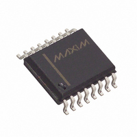
MAX187BCWE+ Maxim Integrated Products, MAX187BCWE+ Datasheet - Page 4

MAX187BCWE+
Manufacturer Part Number
MAX187BCWE+
Description
IC ADC SRL12BIT 5V 75KSPS 16SOIC
Manufacturer
Maxim Integrated Products
Datasheet
1.MAX189CCPA.pdf
(20 pages)
Specifications of MAX187BCWE+
Number Of Bits
12
Sampling Rate (per Second)
75k
Data Interface
MICROWIRE™, QSPI™, Serial, SPI™
Number Of Converters
1
Power Dissipation (max)
478mW
Voltage Supply Source
Single Supply
Operating Temperature
0°C ~ 70°C
Mounting Type
Surface Mount
Package / Case
16-SOIC (0.300", 7.50mm Width)
Number Of Adc Inputs
1
Architecture
SAR
Conversion Rate
75 KSPs
Resolution
12 bit
Input Type
Voltage
Interface Type
Serial
Voltage Reference
Internal 4.096 V
Supply Voltage (max)
5 V
Maximum Power Dissipation
478 mW
Maximum Operating Temperature
+ 70 C
Mounting Style
SMD/SMT
Minimum Operating Temperature
0 C
Lead Free Status / RoHS Status
Lead free / RoHS Compliant
ELECTRICAL CHARACTERISTICS (continued)
(V
reference: V
capacitor at REF pin; T
+5V, Low-Power, 12-Bit Serial ADCs
4
DIGITAL INPUTS (SCLK,
SCLK, CS Input High Voltage
SCLK, CS Input Low Voltage
SCLK, CS Input Hysteresis
SCLK, CS Input Leakage
SCLK, CS Input Capacitance
SHDN Input High Voltage
SHDN Input Low Voltage
SHDN Input Current
SHDN Input Mid Voltage
SHDN Voltage, Floating
SHDN Maximum Allowed
Leakage, Mid Input
DIGITAL OUTPUT (DOUT)
Output Voltage Low
Output Voltage High
Three-State Leakage Current
Three-State Output
Capacitance
POWER REQUIREMENTS
Supply Voltage
Supply Current
Power-Supply Rejection
DD
_______________________________________________________________________________________
= +5V ±5%; GND = 0V; unipolar input mode; 75ksps, f
PARAMETER
REF
= 4.096V, 4.7µF capacitor at REF pin, or MAX189—external reference: V
A
= T
CS
MIN
,
SHDN
to T
SYMBOL
V
V
V
C
V
V
V
V
PSR
V
V
MAX
C
I
V
HYST
I
INSH
I
INSL
INS
OUT
DD
INH
FLT
I
INL
OH
IN
OL
DD
IM
)
L
IN
; unless otherwise noted.)
V
(Note 4)
SHDN = V
SHDN = open
SHDN = open
I
I
I
CS = 5V
CS = 5V (Note 4)
Operating mode
Power-down mode
V
full-scale input (Note 6)
SINK
SINK
SOURCE
IN
DD
= 0V or V
= +5V, ±5%; external reference, 4.096V;
= 5mA
= 16mA
= 1mA
DD
or 0V
DD
CONDITIONS
CLK
= 4.0MHz, external clock (50% duty cycle); MAX187—internal
MAX187
MAX189
V
REF
DD
MIN
-100
4.75
2.4
1.5
4
- 0.5
= 4.096V applied to REF pin, 4.7µF
±0.06
0.15
2.75
TYP
0.3
1.5
1.0
2
V
DD
MAX
±4.0
±0.5
5.25
100
±10
0.8
0.5
0.4
2.5
2.0
±1
15
15
10
-1.5
UNITS
mA
mV
µA
pF
µA
nA
µA
pF
µA
V
V
V
V
V
V
V
V
V
V


