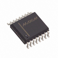
MAX187BCWE+ Maxim Integrated Products, MAX187BCWE+ Datasheet - Page 9

MAX187BCWE+
Manufacturer Part Number
MAX187BCWE+
Description
IC ADC SRL12BIT 5V 75KSPS 16SOIC
Manufacturer
Maxim Integrated Products
Datasheet
1.MAX189CCPA.pdf
(20 pages)
Specifications of MAX187BCWE+
Number Of Bits
12
Sampling Rate (per Second)
75k
Data Interface
MICROWIRE™, QSPI™, Serial, SPI™
Number Of Converters
1
Power Dissipation (max)
478mW
Voltage Supply Source
Single Supply
Operating Temperature
0°C ~ 70°C
Mounting Type
Surface Mount
Package / Case
16-SOIC (0.300", 7.50mm Width)
Number Of Adc Inputs
1
Architecture
SAR
Conversion Rate
75 KSPs
Resolution
12 bit
Input Type
Voltage
Interface Type
Serial
Voltage Reference
Internal 4.096 V
Supply Voltage (max)
5 V
Maximum Power Dissipation
478 mW
Maximum Operating Temperature
+ 70 C
Mounting Style
SMD/SMT
Minimum Operating Temperature
0 C
Lead Free Status / RoHS Status
Lead free / RoHS Compliant
Figure 3a. MAX187 Operational Diagram
ANALOG INPUT
Figure 4. Equivalent Input Circuit
In track mode, the analog signal is acquired and stored
in the internal hold capacitor. In hold mode, the T/H
switch opens and maintains a constant input to the
ADC’s SAR section.
During acquisition, the analog input AIN charges
capacitor C
C PACKAGE
SHUTDOWN
OFF
0V TO +5V
GND
AIN
INPUT
4.7 F
ON
REF
TRACK INPUT
+5V
HOLD
HOLD
12-BIT CAPACITIVE DAC
. Bringing CS low ends the acquisition
_______________________________________________________________________________________
C SWITCH
1
2
3
4
C HOLD
-
16pF
TRACK
V DD
AIN
SHDN
REF
+
MAX187
4.7 F
0.1 F
R
5k
IN
+5V, Low-Power, 12-Bit Serial ADCs
HOLD
DOUT
SCLK
ZERO
GND
CS
8
7
6
5
AT THE SAMPLING INSTANT,
THE INPUT SWITCHES FROM
AIN TO GND.
COMPARATOR
Track/Hold
SERIAL
INTERFACE
interval. At this instant, the T/H switches the input side
of C
resents a sample of the input, unbalancing the node
ZERO at the comparator’s input.
In hold mode, the capacitive DAC adjusts during the
remainder of the conversion cycle to restore node
ZERO to 0V within the limits of a 12-bit resolution. This
action is equivalent to transferring a charge from
C
turn forms a digital representation of the analog input
signal. At the conversion’s end, the input side of C
switches back to AIN, and C
signal again.
The time required for the T/H to acquire an input signal
is a function of how quickly its input capacitance is
charged. If the input signal’s source impedance is
high, the acquisition time lengthens and more time
must be allowed between conversions. Acquisition time
is calculated by:
where R
input signal, and t
impedances below 5kΩ do not significantly affect the
AC performance of the ADC.
Figure 3b. MAX189 Operational Diagram
ANALOG INPUT
HOLD
SHUTDOWN
REFERENCE
OFF
0V TO +5V
HOLD
INPUT
INPUT
to the binary-weighted capacitive DAC, which in
IN
0.1 F
to GND. The retained charge on C
ON
= 5kΩ, R
+5V
t
ACQ
ACQ
= 9 (R
1
2
3
4
S
= the source impedance of the
is never less than 1.5µs. Source
V DD
AIN
SHDN
REF
S
MAX189
4.7 F
0.1 F
+ R
HOLD
IN
DOUT
SCLK
GND
) 16pF,
CS
charges to the input
8
7
6
5
HOLD
SERIAL
INTERFACE
HOLD
rep-
9


