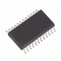
MAX132CWG+ Maxim Integrated Products, MAX132CWG+ Datasheet - Page 13

MAX132CWG+
Manufacturer Part Number
MAX132CWG+
Description
IC ADC 18BIT W/SRL INTRFC 24SOIC
Manufacturer
Maxim Integrated Products
Datasheet
1.MAX132CNG.pdf
(16 pages)
Specifications of MAX132CWG+
Number Of Bits
18
Sampling Rate (per Second)
100
Data Interface
MICROWIRE™, Serial, SPI™
Number Of Converters
1
Voltage Supply Source
Dual ±
Operating Temperature
0°C ~ 70°C
Mounting Type
Surface Mount
Package / Case
24-SOIC (0.300", 7.50mm Width)
Architecture
Dual Slope
Conversion Rate
0.1 KSPs
Input Type
Voltage
Interface Type
4-Wire (SPI, QSPI, MICROWIRE, TMS320)
Supply Voltage (max)
5 V
Maximum Power Dissipation
647 mW
Maximum Operating Temperature
+ 70 C
Mounting Style
SMD/SMT
Minimum Operating Temperature
0 C
Lead Free Status / RoHS Status
Lead free / RoHS Compliant
read, the collision bit is automatically reset to 0. To deter-
mine collision status, read the status register collision bit
before and after reading output registers 0 and 1.
Collisions will not occur if a conversion’s read cycle is
completed before the next conversion begins.
A binary sequencing counter controls the conversion
phase’s sequencing (or timing). In integrate phase,
both start and stop occur at preset counts. The deinte-
gration phases start at predetermined counts, but are
terminated when the comparator detects zero crossing
at the integrator output.
The results counter accumulates counts during all dein-
tegrate phases. It is an up/down binary counter, with
the count direction determined by the deintegration
polarity. In the first deintegrate phase, the results
counter counts by 512. Since the second deintegrate
phase deintegrates a residual voltage multiplied by 8,
the results counter increments or decrements by 64
during this phase. It increments or decrements by 8
during the third deintegrate phase, and by 1 during the
fourth deintegrate phase. The results counter content
transfers to the results register at each conversion end.
B18 is not strictly an overrange bit. This 19th bit is nec-
essary to exploit the converter’s full range, and to
ensure that a full 18-bit result can be achieved after a
zero reading has been deducted.
The actual overrange value is a function of the number
of bits of resolution used. Table 4 lists the overrange
values for different resolutions.
The MAX132 has two overrange levels (Figure 10 and
Table 4). The first level is a soft overrange that is set by
the user. Overrange is arbitrarily set at a value, prefer-
ably less than the 279,040 (including any zero offset)
raw counts soft limit. A nonlinearity step of about 64
counts occurs at raw count 279,040 and again at
330,240 counts.
The second level is a hard overrange with a maximum
value of 350,440 counts. Attempts to deintegrate values
greater than this will result in a value of ±350,440 counts.
Multislope conversion allows 350,440 counts with a clock
frequency of only 32.768kHz. After zero-crossing, the
main comparator (with some delay) sends a signal to the
digital control section, which then terminates the deinte-
grate period by issuing commands to the analog switch-
es. This action entails further delay because the
____Multislope Conversion Phases
Sequence Counter and Results Counter
______________________________________________________________________________________
Overrange Indication
±18-Bit ADC with Serial Interface
commands must be synchronous with the clock. As a
result, the delay between zero-crossing and switch actu-
ation can exceed one clock cycle. A “residue” voltage
that represents unwanted extra counts in the conversion
result is left on the capacitor, while the integrator’s output
continues past the zero crossing.
Dual-slope converters ignore this residue voltage error.
However, the multislope MAX132 inverts, amplifies, and
deintegrates the residue, canceling the extra counts by
driving an up/down counter in the opposite direction.
This process of measuring and accounting for the residue
can be repeated for the successively smaller errors
remaining after each deintegration. (Deintegration is sim-
ply an integration of V
grator output ramps toward zero.) The MAX132, for
example, executes three cycles in which the residue is
inverted, multiplied by eight, and deintegrated (Figure 10).
The MAX132 integrates the input signal by connecting
the integrator’s noninverting input to IN LO, and the
buffer input to IN Hl. The integration period is 545
counts for 60Hz mode and 655 counts for 50Hz
The integrator capacitor’s voltage polarity at the end of
integrate phase determines the polarity of the first dein-
tegration phase. The first deintegration phase ends
when the comparator detects that the integration
capacitor has been discharged. The MAX132 then
goes into a rest phase, where both the buffer input and
the integrator’s noninverting input are connected to
AGND, integrating the system offset.
Near the end of the maximum allowable deintegration
period, the integrator capacitor voltage polarity is again
sampled, resulting in either a positive or negative dein-
tegrate cycle.
A rest phase follows each deintegrate phase. The rest
phase starts when the integrator crosses zero and ends
when the maximum count for that deintegration phase
has been reached.
When the zero crossing is detected at the end of the
deintegrate phase, deintegration continues until the
next clock cycle. This causes the integrator to over-
shoot zero crossing slightly, leaving a small residual
voltage on the integration capacitor. The first times-
eight (X8) phase inverts and multiplies this residual by
a factor of 8.
REF
, with polarity chosen so the inte-
First Times-Eight Phase
Deintegrate Phase
Integrate Phase
Rest Phase
13


