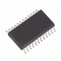
MAX132CWG+ Maxim Integrated Products, MAX132CWG+ Datasheet - Page 6

MAX132CWG+
Manufacturer Part Number
MAX132CWG+
Description
IC ADC 18BIT W/SRL INTRFC 24SOIC
Manufacturer
Maxim Integrated Products
Datasheet
1.MAX132CNG.pdf
(16 pages)
Specifications of MAX132CWG+
Number Of Bits
18
Sampling Rate (per Second)
100
Data Interface
MICROWIRE™, Serial, SPI™
Number Of Converters
1
Voltage Supply Source
Dual ±
Operating Temperature
0°C ~ 70°C
Mounting Type
Surface Mount
Package / Case
24-SOIC (0.300", 7.50mm Width)
Architecture
Dual Slope
Conversion Rate
0.1 KSPs
Input Type
Voltage
Interface Type
4-Wire (SPI, QSPI, MICROWIRE, TMS320)
Supply Voltage (max)
5 V
Maximum Power Dissipation
647 mW
Maximum Operating Temperature
+ 70 C
Mounting Style
SMD/SMT
Minimum Operating Temperature
0 C
Lead Free Status / RoHS Status
Lead free / RoHS Compliant
The MAX132 integrates the input voltage for a fixed
period of time, then deintegrates a known reference
voltage and measures the time required to reach zero.
Good line rejection is achieved by setting the (input)
integration time equal to one 50Hz or 60Hz period. The
MAX132 has a 50Hz/60Hz mode selection bit that sets
the integration time to 655/545 clock periods, respec-
tively, so that 50Hz/60Hz rejection is obtained with a
32,768Hz crystal. The MAX132 is tested and guaran-
teed at a 16 conv/sec throughput rate. Figure 1 shows
the basic MAX132 application circuit, with component
values selected for 16 conv/sec .
For applications that don’t require 50Hz/60Hz rejection,
the MAX132 will operate up to 100 conv/sec at reduced
accuracy (typically 0.012% FSR nonlinearity, or ±13
bits). In these applications, the 50Hz mode is recom-
mended because of its longer (655 count) integration
time. See Increased Speed section.
±18-Bit ADC with Serial Interface
Figure 2. Serial-Mode Timing
Figure 3. Load Circuits for Access Time
6
____________Functional Description
DOUT
_______________________________________________________________________________________
P0–P3
DOUT
SCLK
DIN
CS
3k
a. High-Z to V
DGND
OH
t
8
(t
8
)
t
1
C
L
t
6
MSB IN
MSB OUT
DOUT
t
7
t
3
b. High-Z to V
+5V
t
4
3k
OL
C
DGND
L
(t
8
)
B6–B1
B6–B1
The recommended analog full-scale input range is
±512mV. Performance is tested and guaranteed at
±512mV full scale, corresponding to a 2µV/LSB resolu-
tion at 18 bits. Resolution is defined as follows:
which corresponds to 2µV/LSB resolution at 18 bits.
Consult the Typical Operating Characteristics for Noise
vs. Number of Samples Averaged and other important
operating parameters. Note how accuracy depends on
common-mode input voltage (common mode is defined
here as
set the analog input full-scale between ±470mV and
__________Analog Design Procedure
Figure 4. Load Circuits for Disable Time to Three-State
DOUT
Re
solution Volts LSB
|
3k
V
LSB IN
IN
a. V
LSB OUT
OH
LO - AGND
to High-Z (t
DGND
t
10
9
/
)
t
10pF
2
|
). For optimum performance,
and Input Protection
Input Voltage Range
t
11
t
10
, t
DOUT
V
12
t
IN
5
(
FS
b. V
) /
OL
to High-Z (t
262 144
+5V
,
3k
10pF
DGND
10
)


