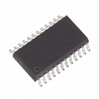
MAX132CWG+ Maxim Integrated Products, MAX132CWG+ Datasheet - Page 14

MAX132CWG+
Manufacturer Part Number
MAX132CWG+
Description
IC ADC 18BIT W/SRL INTRFC 24SOIC
Manufacturer
Maxim Integrated Products
Datasheet
1.MAX132CNG.pdf
(16 pages)
Specifications of MAX132CWG+
Number Of Bits
18
Sampling Rate (per Second)
100
Data Interface
MICROWIRE™, Serial, SPI™
Number Of Converters
1
Voltage Supply Source
Dual ±
Operating Temperature
0°C ~ 70°C
Mounting Type
Surface Mount
Package / Case
24-SOIC (0.300", 7.50mm Width)
Architecture
Dual Slope
Conversion Rate
0.1 KSPs
Input Type
Voltage
Interface Type
4-Wire (SPI, QSPI, MICROWIRE, TMS320)
Supply Voltage (max)
5 V
Maximum Power Dissipation
647 mW
Maximum Operating Temperature
+ 70 C
Mounting Style
SMD/SMT
Minimum Operating Temperature
0 C
Lead Free Status / RoHS Status
Lead free / RoHS Compliant
The second deintegrate phase deintegrates residual
voltage on the integration capacitor that has been
through the X8 phase. Since the voltage across the
integration capacitor has been multiplied by 8, each
deintegration clock cycle corresponds to 1/8 of one
clock cycle during the first deintegration.
At the end of the second and third deintegration phas-
es, the device performs a X8 multiplication of the resid-
ual voltage left on the integration capacitor. After each
of these X8 multiplications, a deintegration occurs,
resulting in a second, third, and fourth deintegration
phase. Each time the residual voltage on the integration
capacitor is multiplied by 8, the following deintegration
has 8 times finer resolution.
The zero-integrate phase zeros out the integrator to
prepare for the next integration (Figure 10). This phase
occurs at the beginning and end of each conversion. At
power-up, or in the hold mode prior to a conversion, the
MAX132 continues to zero integrate until a conversion
starts. When a conversion starts in 60Hz mode, another
111 clocks of zero integrate are completed before the
beginning of a conversion. In 50Hz mode, only one
additional zero integrate is performed before the con-
version starts. An additional 20 clocks of zero integrate
occur at each conversion end.
An extended delay between conversions can degrade
the subsequent conversion result due to capacitor
droop and internal offset/common-mode voltages. The
initial reading may be off by 4 to 6 counts in a ±15-bit
configuration. When the delay between conversions
exceeds 2 seconds (either because of a slower conver-
sion rate or the use of sleep mode), it is recommended
that the first reading after this delay be discarded.
The MAX132 is tested with a 32,768Hz clock frequen-
cy, which results in 16 conv/sec. Up to 96 conv/sec
may be achieved with higher clock frequencies and
some changes in component values, as shown in Table
1. Operation at higher conversion rates reduces accu-
racy, and care must be taken to get the best results.
±18-Bit ADC with Serial Interface
14
__________Applications Information
Extended Delays Between Conversions
______________________________________________________________________________________
Second Deintegrate Phase
and Deintegrate Phases
Additional Times-Eight
Zero-Integrate Phase
Increased Speed
Although either the 50Hz or 60Hz mode can be used,
complete rejection of 50Hz or 60Hz normal-mode noise
at conversion rates above 16 conv/sec is impossible.
Use the 50Hz mode when operating at more than 16
conv/sec, irrespective of the local line frequency. The
50Hz mode uses a slightly longer integration time than
the 60Hz mode, and generally gives lower-noise perfor-
mance.
Table 1 lists the crystal frequencies and integrating
capacitor values for the 50Hz and 60Hz modes for vari-
ous conversion rates, although the 50Hz mode is rec-
ommended for clock rates above 32,768Hz.
The raw data can be used where highest accuracy is
not required, and the least significant bits can be
ignored. At 96 conv/sec, the accuracy is 13 bits.
Improvements in accuracy can be gained by averaging
both the data and the zero readings, although data
averaging compromises the converter’s speed perfor-
mance.
To maximize throughput, take zero readings only when
necessary, i.e., when the common-mode voltage
changes. It is not normally necessary to take a zero read-
ing after every data reading‚ as an excessive number of
zero readings reduces the converter’s effective speed.
To minimize noise, each supply must be bypassed to
GND with a 0.1µF capacitor. A ground plane should
also be placed under the analog circuitry. Use the RC
network at the inputs as shown in Figure 6. Also refer to
the section “Noise Reduction Techniques” in the notes
for the MAX132 evaluation kit. To minimize the coupling
effects of stray capacitance, keep digital lines as far
from analog components and lines as possible. Also,
connect the integrator capacitor’s outside foil to the INT
OUT pin to minimize stray capacitive coupling. If possi-
ble, keep the digital interface inactive while the
MAX132 is converting.
Figure 11 shows an application to measure tempera-
ture ratiometrically with an RTD sensor. The voltage
drops across the RTD sensor and the 250Ω reference
resistor are generated by the same current source. The
voltage of the sensor (V
ential inputs, and the voltage drop across the reference
resistor (V
inputs. The relationship of these voltages is ratiometric
and unaffected by the actual current. The MAX132’s
output is proportional to V
R
) is brought into the differential reference
Ratiometric Measurements
S
) is fed directly into the differ-
S
divided by V
Noise Reduction
R
, independent


