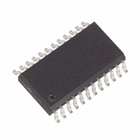
MAX132CWG+ Maxim Integrated Products, MAX132CWG+ Datasheet - Page 8

MAX132CWG+
Manufacturer Part Number
MAX132CWG+
Description
IC ADC 18BIT W/SRL INTRFC 24SOIC
Manufacturer
Maxim Integrated Products
Datasheet
1.MAX132CNG.pdf
(16 pages)
Specifications of MAX132CWG+
Number Of Bits
18
Sampling Rate (per Second)
100
Data Interface
MICROWIRE™, Serial, SPI™
Number Of Converters
1
Voltage Supply Source
Dual ±
Operating Temperature
0°C ~ 70°C
Mounting Type
Surface Mount
Package / Case
24-SOIC (0.300", 7.50mm Width)
Architecture
Dual Slope
Conversion Rate
0.1 KSPs
Input Type
Voltage
Interface Type
4-Wire (SPI, QSPI, MICROWIRE, TMS320)
Supply Voltage (max)
5 V
Maximum Power Dissipation
647 mW
Maximum Operating Temperature
+ 70 C
Mounting Style
SMD/SMT
Minimum Operating Temperature
0 C
Lead Free Status / RoHS Status
Lead free / RoHS Compliant
±18-Bit ADC with Serial Interface
The main source of rollover voltage error is due to
common-mode voltages. This error is caused by the
reference capacitor losing or gaining charge to stray
capacitance. A positive signal with a large common-
mode voltage can cause the reference capacitor to
gain charge (increase voltage). In contrast, the refer-
ence capacitor will lose charge (decrease voltage)
when deintegrating a negative input signal. Rollover
error is a direct result of the difference in reference to
positive or negative input voltages. With the recom-
mended reference capacitor types, the worst-case
rollover error is 0.01% of full-scale. Connect REF- to
AGND to minimize rollover error. As outlined in the ref-
erence section, reference voltages below 500mV also
contribute to rollover errors.
Figure 6. MAX132 Input Circuit
Figure 7. Dividing MAX872 to Generate the MAX132’s
Reference Voltage
8
±512mV
_______________________________________________________________________________________
REF+
REF-
100k
0.1 F
1 F
Differential Reference Inputs
14
15
16
17
IN HI
IN LO
AGND
REF-
120k
100k
40.2k
MAX132
and Rollover Error
+5V
-5V
V+
V-
MAX872
24
13
+5V
2.5V
REF+
18
+545mV
The internal oscillator is typically driven by a crystal, as
shown in Figure 8, or by an external clock. If an exter-
nal clock is used, connect the clock to OSC1 and leave
OSC2 floating. The duty-cycle can vary from 20% to
80%. The typical threshold voltage is approximately 2V.
For proper start-up, a full +5V CMOS-logic swing is
required.
The oscillator frequency sets the conversion rate. Use
32,768Hz for applications that require 50Hz or 60Hz
line rejection. This frequency yields 16 conv/sec. The
same clock frequency can be used to reject both line
frequencies because the MAX132 integrates for a dif-
ferent number of clock cycles in its 50Hz and 60Hz
modes. In each case, the MAX132 integrates for a sin-
gle complete line cycle (20ms for the 50Hz mode,
16.67ms for the 60Hz mode). Refer to the Increased
Speed section for operation at higher conversion rates.
The MAX132 requires an integrator resistor (R
capacitor (C
crystal. All MAX132 tests are performed with a
32,768Hz crystal frequency. The crystal frequency, ref-
erence voltage, and integrator current determine the
values of R
Figure 8 shows the internal oscillator drive circuitry used
with external crystals. The two external capacitors provide
DC bias at start-up. The 15pF capacitors shown are typical
values. The actual capacitance will vary, depending on the
crystal manufacturer’s recommendation and board layout.
Figure 8. MAX132 Internal Oscillator Drive Circuitry
15pF
5pF
INT
INT
and C
), a reference capacitor (C
OSC1
6
INT
1M
.
150k
External Components
OSC2
5
5pF
15pF
Oscillator Circuit
+5V
MAX132
REF
INT
), and a
Crystal
) and


