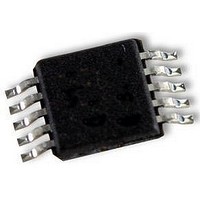
AD5175BRMZ-10 Analog Devices Inc, AD5175BRMZ-10 Datasheet - Page 12

AD5175BRMZ-10
Manufacturer Part Number
AD5175BRMZ-10
Description
IC DGTL POT 1024POS 10K 10MSOP
Manufacturer
Analog Devices Inc
Datasheet
1.AD5175BRMZ-10-RL7.pdf
(20 pages)
Specifications of AD5175BRMZ-10
Taps
1024
Resistance (ohms)
10K
Number Of Circuits
1
Temperature Coefficient
35 ppm/°C Typical
Memory Type
Non-Volatile
Interface
I²C, 2-Wire Serial
Voltage - Supply
2.7 V ~ 5.5 V, ±2.5 V ~ 2.75 V
Operating Temperature
-40°C ~ 125°C
Mounting Type
Surface Mount
Package / Case
10-MSOP, Micro10™, 10-uMAX, 10-uSOP
Resistance In Ohms
10K
End To End Resistance
10kohm
Resistance Tolerance
-15% To +15%
No. Of Steps
1024
Supply Voltage Range
2.7V To 5.5V, ± 2.7V
Control Interface
I2C, Serial
No. Of Pots
Single
Memory
RoHS Compliant
Rohs Compliant
Yes
Lead Free Status / RoHS Status
Lead free / RoHS Compliant
Available stocks
Company
Part Number
Manufacturer
Quantity
Price
Company:
Part Number:
AD5175BRMZ-10
Manufacturer:
VISHAY
Quantity:
5 015
Part Number:
AD5175BRMZ-10
Manufacturer:
ADI/亚德诺
Quantity:
20 000
Part Number:
AD5175BRMZ-10-RL7
Manufacturer:
ADI/亚德诺
Quantity:
20 000
AD5175
THEORY OF OPERATION
The AD5175 is designed to operate as a true variable resistor for
analog signals within the terminal voltage range of V
< V
position. The RDAC register acts as a scratchpad register, which
allows unlimited changes of resistance settings. The RDAC
register can be programmed with any position setting using
the I
value can be stored in a 50-TP memory register. Thereafter, the
wiper position is always restored to that position for subsequent
power-up. The storing of 50-TP data takes approximately 350 ms;
during this time, the AD5175 is locked and does not acknowl-
edge any new command thereby preventing any changes from
taking place. The acknowledge bit can be polled to verify that
the fuse program command is complete.
SERIAL DATA INTERFACE
The AD5175 has a 2-wire I
It can be connected to an I
control of a master device; see Figure 3 for a timing diagram
of a typical write sequence.
The AD5175 supports standard (100 kHz) and fast (400 kHz)
data transfer modes. Support is not provided for 10-bit
addressing and general call addressing.
The AD5175 has a 7-bit slave address. The five MSBs are 01011
and the two LSBs are determined by the state of the ADDR pin.
The facility to make hardwired changes to ADDR allows the
user to incorporate up to three of these devices on one bus, as
outlined in Table 6.
Table 6. Device Address Selection
ADDR Pin
GND
V
NC (No Connection)
1
Not available in bipolar mode. V
DD
DD
2
C interface. When a desirable wiper position is found, this
. The RDAC register contents determine the resistor wiper
1
2
2
C bus as a slave device under the
SS
C-compatible serial interface.
< 0 V.
A1
1
0
1
SS
< V
TERM
Rev. A | Page 12 of 20
The 2-wire serial bus protocol operates as follows: The master
initiates a data transfer by establishing a start condition, which
is when a high-to-low transition on the SDA line occurs while
SCL is high. The next byte is the address byte, which consists
of the 7-bit slave address and a R/ W bit. The slave device
corresponding to the transmitted address responds by pulling
SDA low during the ninth clock pulse (this is termed the acknowl-
edge bit). At this stage, all other devices on the bus remain idle
while the selected device waits for data to be written to, or read
from, its shift register.
Data is transmitted over the serial bus in sequences of nine
clock pulses (eight data bits followed by an acknowledge bit).
The transitions on the SDA line must occur during the low
period of SCL and remain stable during the high period of SCL.
When all data bits have been read or written, a stop condition is
established. In write mode, the master pulls the SDA line high
during the 10
mode, the master issues a no acknowledge for the ninth clock
pulse, that is, the SDA line remains high. The master then
brings the SDA line low before the 10
high during the 10
SHIFT REGISTER
For the AD5175, the shift register is 16 bits wide, as shown in
Figure 2. The 16-bit word consists of two unused bits, which
should be set to 0, followed by four control bits and 10 RDAC data
bits, and data is loaded MSB first (Bit D9). The four control bits
determine the function of the software command (Table 7).
sequence.
The command bits (Cx) control the operation of the digital
potentiometer and the internal 50-TP memory. The data bits
(Dx) are the values that are loaded into the decoded register.
Figure 25 shows a timing diagram of a typical AD5175 write
A0
1
0
0
th
clock pulse to establish a stop condition. In read
th
clock pulse to establish a stop condition.
7-Bit I
0101111
0101100
0101110
th
clock pulse, and then
2
C Device Address


