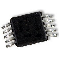
AD5175BRMZ-10 Analog Devices Inc, AD5175BRMZ-10 Datasheet - Page 15

AD5175BRMZ-10
Manufacturer Part Number
AD5175BRMZ-10
Description
IC DGTL POT 1024POS 10K 10MSOP
Manufacturer
Analog Devices Inc
Datasheet
1.AD5175BRMZ-10-RL7.pdf
(20 pages)
Specifications of AD5175BRMZ-10
Taps
1024
Resistance (ohms)
10K
Number Of Circuits
1
Temperature Coefficient
35 ppm/°C Typical
Memory Type
Non-Volatile
Interface
I²C, 2-Wire Serial
Voltage - Supply
2.7 V ~ 5.5 V, ±2.5 V ~ 2.75 V
Operating Temperature
-40°C ~ 125°C
Mounting Type
Surface Mount
Package / Case
10-MSOP, Micro10™, 10-uMAX, 10-uSOP
Resistance In Ohms
10K
End To End Resistance
10kohm
Resistance Tolerance
-15% To +15%
No. Of Steps
1024
Supply Voltage Range
2.7V To 5.5V, ± 2.7V
Control Interface
I2C, Serial
No. Of Pots
Single
Memory
RoHS Compliant
Rohs Compliant
Yes
Lead Free Status / RoHS Status
Lead free / RoHS Compliant
Available stocks
Company
Part Number
Manufacturer
Quantity
Price
Company:
Part Number:
AD5175BRMZ-10
Manufacturer:
VISHAY
Quantity:
5 015
Part Number:
AD5175BRMZ-10
Manufacturer:
ADI/亚德诺
Quantity:
20 000
Part Number:
AD5175BRMZ-10-RL7
Manufacturer:
ADI/亚德诺
Quantity:
20 000
READ OPERATION
When reading data back from the AD5175, the user must first
issue a readback command to the device, this begins with a start
command followed by an address byte (R/ W = 0), after which
the AD5175 acknowledges that it is prepared to receive data by
pulling SDA low.
Two bytes of data are then written to the AD5175, the most
significant byte followed by the least significant byte; both
of these data bytes are acknowledged by the AD5175. A stop
condition follows. These bytes contain the read instruction,
SDA
SDA
SCL
SCL
START BY
START BY
MASTER
MASTER
0
1
0
1
1
1
SERIAL BUS ADDRESS BYTE
SERIAL BUS ADDRESS BYTE
0
0
SDA (CONTINUED)
SDA (CONTINUED)
SCL (CONTINUED)
SCL (CONTINUED)
FRAME 1
FRAME 1
1
1
1
1
A1
A1
A0
A0
Figure 27. Read Command
R/W
R/W
9
Rev. A | Page 15 of 20
9
ACK. BY
AD5175
ACK. BY
AD5175
D7
1
9
D7
1
9
D6
1
0
D6
0
1
which enables readback of the RDAC register, 50-TP memory,
or the control register. The user can then read back the data
beginning with a start command followed by an address byte
(R/ W = 1), after which the device acknowledges that it is
prepared to transmit data by pulling SDA low. Two bytes of
data are then read from the device, as shown in
stop condition follows. If the master does not acknowledge the
first byte, the second byte is not transmitted by the AD5175.
LEAST SIGNIFICANT DATA BYTE
LEAST SIGNIFICANT DATA BYTE
D5
0
D5
0
D4
X
C3
MOST SIGNIFICANT DATA BYTE
D4
MOST SIGNIFICANT DATA BYTE
FRAME 3
FRAME 3
D3
X
C2
D3
FRAME 2
FRAME 2
D2
X
C1
D2
D1
X
C0
D1
D9
D0
D9
D0
ACK. BY
NO ACK. BY
AD5175
MASTER
D8
9
D8
9
ACK. BY
MASTER
ACK. BY
AD5175
STOP BY
MASTER
STOP BY
MASTER
9
9
Figure 27
AD5175
. A


