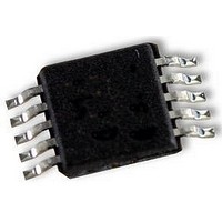
AD5175BRMZ-10 Analog Devices Inc, AD5175BRMZ-10 Datasheet - Page 16

AD5175BRMZ-10
Manufacturer Part Number
AD5175BRMZ-10
Description
IC DGTL POT 1024POS 10K 10MSOP
Manufacturer
Analog Devices Inc
Datasheet
1.AD5175BRMZ-10-RL7.pdf
(20 pages)
Specifications of AD5175BRMZ-10
Taps
1024
Resistance (ohms)
10K
Number Of Circuits
1
Temperature Coefficient
35 ppm/°C Typical
Memory Type
Non-Volatile
Interface
I²C, 2-Wire Serial
Voltage - Supply
2.7 V ~ 5.5 V, ±2.5 V ~ 2.75 V
Operating Temperature
-40°C ~ 125°C
Mounting Type
Surface Mount
Package / Case
10-MSOP, Micro10™, 10-uMAX, 10-uSOP
Resistance In Ohms
10K
End To End Resistance
10kohm
Resistance Tolerance
-15% To +15%
No. Of Steps
1024
Supply Voltage Range
2.7V To 5.5V, ± 2.7V
Control Interface
I2C, Serial
No. Of Pots
Single
Memory
RoHS Compliant
Rohs Compliant
Yes
Lead Free Status / RoHS Status
Lead free / RoHS Compliant
Available stocks
Company
Part Number
Manufacturer
Quantity
Price
Company:
Part Number:
AD5175BRMZ-10
Manufacturer:
VISHAY
Quantity:
5 015
Part Number:
AD5175BRMZ-10
Manufacturer:
ADI/亚德诺
Quantity:
20 000
Part Number:
AD5175BRMZ-10-RL7
Manufacturer:
ADI/亚德诺
Quantity:
20 000
AD5175
RDAC REGISTER
The RDAC register directly controls the position of the digital
rheostat wiper. For example, when the RDAC register is loaded
with all 0s, the wiper is connected to Terminal A of the variable
resistor. It is possible to both write to and read from the RDAC
register using the I
logic register; there is no restriction on the number of changes
allowed.
50-TP MEMORY BLOCK
The AD5175 contains an array of 50-TP programmable
memory registers, which allow the wiper position to be pro-
grammed up to 50 times. Table 11 shows the memory map.
Command 3 in Table 7 programs the contents of the RDAC
register to memory. The first address to be programmed is
Location 0x01, see Table 11, and the AD5175 increments the
50-TP memory address for each subsequent program until
the memory is full. Programming data to 50-TP consumes
approximately 4 mA for 55 ms, and takes approximately
350 ms to complete, during which time the shift register is
locked preventing any changes from taking place. Bit C2 of
the control register in Table 10 can be polled to verify that the
fuse program command was successful. No change in supply
voltage is required to program the 50-TP memory; however, a
1 μF capacitor on the EXT_CAP pin is required as shown in
Figure 29.
Table 7. Command Operation Truth Table
Command
Number
0
1
2
3
4
5
6
7
8
9
1
2
3
X is don’t care.
See Table 11 for the 50-TP memory map.
See Table 10 for bit details.
2
3
C3
0
0
0
0
0
0
0
0
1
1
Command[DB13:DB10]
2
C interface. The RDAC register is a standard
C2
0
0
0
0
1
1
1
1
0
0
C1
0
0
1
1
0
0
1
1
0
0
C0
0
1
0
1
0
1
0
1
0
1
D9
X
D9
X
X
X
X
X
X
X
X
D8
X
D8
X
X
X
X
X
X
X
X
D7
X
D7
X
X
X
X
X
X
X
X
D6
D6
X
X
X
X
X
X
X
X
X
Rev. A | Page 16 of 20
Data[DB9:DB0]
D5
X
D5
X
X
X
D5
X
X
X
X
D4
X
D4
X
X
X
X
X
X
X
D4
Prior to 50-TP activation, the AD5175 presets to midscale on
power-up. It is possible to read back the contents of any of the
50-TP memory registers through the I
Command 5 in Table 7. The lower six LSB bits, D0 to D5 of
the data byte, select which memory location is to be read back.
A binary encoded version address of the most recently pro-
grammed wiper memory location can be read back using
Command 6 in Table 7. This can be used to monitor the
spare memory status of the 50-TP memory block.
WRITE PROTECTION
On power-up, serial data input register write commands for
both the RDAC register and the 50-TP memory registers are
disabled. The RDAC write protect bit (Bit C1) of the control
register (see Table 9 and Table 10), is set to 0 by default. This
disables any change of the RDAC register content regardless
of the software commands, except that the RDAC register can
be refreshed from the 50-TP memory using the software reset,
Command 4, or through the hardware by the RESET pin. To
enable programming of the variable resistor wiper position
(programming the RDAC register), the write protect bit
(Bit C1) of the control register must first be programmed.
This is accomplished by loading the serial data input register
with Command 7 (see
50-TP memory block, Bit C0 of the control register, which is set
to 0 by default, must first be set to 1.
D3
X
D3
X
X
X
X
X
X
D3
X
1
D2
X
D2
X
X
X
X
X
X
D2
X
D1
X
D1
X
X
X
D1
X
X
X
D1
D0
X
D
X
X
X
D0
X
D0
X
D0
Table 7
Operation
NOP: do nothing.
Write contents of serial register data
to RDAC.
Read contents of RDAC wiper register.
Store wiper setting: store RDAC setting
to 50-TP.
Software reset: refresh RDAC with the
last 50-TP memory stored value.
Read contents of 50-TP from the SDO
output in the next frame.
Read address of the last 50-TP
programmed memory location.
Write contents of the serial register data
to the control register.
Read contents of the control register.
Software shutdown.
D0 = 0; normal mode.
D0 = 1; shutdown mode.
). To enable programming of the
2
C interface by using


