AD5175BRMZ-10 Analog Devices Inc, AD5175BRMZ-10 Datasheet - Page 19
AD5175BRMZ-10
Manufacturer Part Number
AD5175BRMZ-10
Description
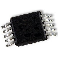
IC DGTL POT 1024POS 10K 10MSOP
Manufacturer
Analog Devices Inc
Datasheet
1.AD5175BRMZ-10-RL7.pdf
(20 pages)
Specifications of AD5175BRMZ-10
Taps
1024
Resistance (ohms)
10K
Number Of Circuits
1
Temperature Coefficient
35 ppm/°C Typical
Memory Type
Non-Volatile
Interface
I²C, 2-Wire Serial
Voltage - Supply
2.7 V ~ 5.5 V, ±2.5 V ~ 2.75 V
Operating Temperature
-40°C ~ 125°C
Mounting Type
Surface Mount
Package / Case
10-MSOP, Micro10™, 10-uMAX, 10-uSOP
Resistance In Ohms
10K
End To End Resistance
10kohm
Resistance Tolerance
-15% To +15%
No. Of Steps
1024
Supply Voltage Range
2.7V To 5.5V, ± 2.7V
Control Interface
I2C, Serial
No. Of Pots
Single
Memory
RoHS Compliant
Rohs Compliant
Yes
Lead Free Status / RoHS Status
Lead free / RoHS Compliant
Available stocks
Company
Part Number
Manufacturer
Quantity
Price
Company:

Part Number:
AD5175BRMZ-10
Manufacturer:
VISHAY
Quantity:
5 015
Part Number:
AD5175BRMZ-10
Manufacturer:
ADI/亚德诺
Quantity:
20 000
Part Number:
AD5175BRMZ-10-RL7
Manufacturer:
ADI/亚德诺
Quantity:
20 000


Calculate the Actual End-to-End Resistance
The resistance tolerance is stored in the internal memory
during factory testing. The actual end-to-end resistance
can, therefore, be calculated (which is valuable for calibration,
tolerance matching, and precision applications).
The resistance tolerance in percentage is stored in fixed-point
format, using a 16-bit sign magnitude binary. The sign bit(0 =
negative and 1 = positive) and the integer part is located in
Address 0x39, as shown in Table 11. Address 0x3A contains
the fractional part, as shown in Table 12.
That is, if the data readback from Address 0x39 is 0000001010
and data from Address 0x3A is 0010110000, then the end-to-end
resistance can be calculated as follows.
For Memory Location 0x39,
DB[9:8]: XX = don’t care
DB[7]: 0 = negative
DB[6:0]: 0001010 = 10
For Memory Location 0x3A,
DB[9:8]: XX = don’t care
DB[7:0]: 10110000 = 176 × 2
Therefore, tolerance = −10.6875% and R
EXT_CAP CAPACITOR
A 1 μF capacitor to V
(see Figure 29) on power-up and throughout the operation of
the AD5175.
Table 12. End-to-End Resistance Tolerance Bytes
Memory Map Address
0x39
0x3A
1
X is don’t care.
Figure 29. EXT_CAP Hardware Setup
EXT_CAP
SS
1µF
C1
must be connected to the EXT_CAP pin
−8
= 0.6875
AD5175
MEMORY
BLOCK
50-TP
DB9
X
X
V
V
SS
SS
WA
(1023)= 8.931 kΩ.
DB8
X
X
DB7
Sign
2
−1
Rev. A | Page 19 of 20
DB6
2
2
6
−2
TERMINAL VOLTAGE OPERATING RANGE
The positive V
define the boundary conditions for proper 2-terminal digital
resistor operation. Supply signals present on Terminal A and
Terminal W that exceed V
forward-biased diodes (see Figure 30).
The ground pin of the AD5175 is primarily used as a digital
ground reference. To minimize the digital ground bounce, join
the AD5175 ground terminal remotely to the common ground.
The digital input control signals to the AD5175 must be refe-
renced to the device ground pin (GND) and satisfy the logic
level defined in the Specifications section. An internal level
shift circuit ensures that the common-mode voltage range of
the three terminals extends from V
digital input level.
POWER-UP SEQUENCE
Because there are diodes to limit the voltage compliance at
Terminal A and Terminal W (see Figure 30), it is important to
power V
and Terminal W; otherwise, the diode is forward-biased such
that V
sequence is V
order of powering V
as long as they are powered after V
As soon as V
which first sets the RDAC to midscale and then restores the
last programmed 50-TP value to the RDAC register.
DB5
2
2
5
−3
DD
Data Byte
Figure 30. Maximum Terminal Voltages Set by V
/V
DD
/V
SS
are powered unintentionally. The ideal power-up
DD
SS
SS
DD
, GND, V
DB4
2
2
first before applying any voltage to Terminal A
is powered, the power-on preset activates,
4
−4
and negative V
1
A
, V
W
DD
DB3
2
2
, and digital inputs is not important
DD
, digital inputs, V
3
−5
or V
SS
power supplies of the AD5175
SS
DD
SS
are clamped by the internal
DB2
2
2
/V
to V
2
−6
SS
.
DD
, regardless of the
A
, and V
V
V
A
W
DB1
2
2
SS
DD
1
−7
DD
and V
AD5175
W
. The
SS
DB0
2
2
0
−8
Related parts for AD5175BRMZ-10
Image
Part Number
Description
Manufacturer
Datasheet
Request
R

Part Number:
Description:
Low Cost, Laser Trimmed, Precision IC Op Amp
Manufacturer:
AD [Analog Devices]
Datasheet:

Part Number:
Description:
±1.7g Dual-Axis IMEMS Accelerometer Evaluation Board
Manufacturer:
Analog Devices Inc
Datasheet:

Part Number:
Description:
Inertial Sensor Evaluation System
Manufacturer:
Analog Devices Inc
Datasheet:
Part Number:
Description:
Manufacturer:
Analog Devices Inc
Datasheet:
Part Number:
Description:
Manufacturer:
Analog Devices Inc
Datasheet:
Part Number:
Description:
Manufacturer:
Analog Devices Inc
Datasheet:
Part Number:
Description:
Manufacturer:
Analog Devices Inc
Datasheet:
Part Number:
Description:
Manufacturer:
Analog Devices Inc
Datasheet:
Part Number:
Description:
Manufacturer:
Analog Devices Inc
Datasheet:
Part Number:
Description:
Manufacturer:
Analog Devices Inc
Datasheet:
Part Number:
Description:
Manufacturer:
Analog Devices Inc
Datasheet:
Part Number:
Description:
Manufacturer:
Analog Devices Inc
Datasheet:
Part Number:
Description:
Manufacturer:
Analog Devices Inc
Datasheet: