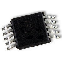
AD5175BRMZ-10 Analog Devices Inc, AD5175BRMZ-10 Datasheet - Page 7

AD5175BRMZ-10
Manufacturer Part Number
AD5175BRMZ-10
Description
IC DGTL POT 1024POS 10K 10MSOP
Manufacturer
Analog Devices Inc
Datasheet
1.AD5175BRMZ-10-RL7.pdf
(20 pages)
Specifications of AD5175BRMZ-10
Taps
1024
Resistance (ohms)
10K
Number Of Circuits
1
Temperature Coefficient
35 ppm/°C Typical
Memory Type
Non-Volatile
Interface
I²C, 2-Wire Serial
Voltage - Supply
2.7 V ~ 5.5 V, ±2.5 V ~ 2.75 V
Operating Temperature
-40°C ~ 125°C
Mounting Type
Surface Mount
Package / Case
10-MSOP, Micro10™, 10-uMAX, 10-uSOP
Resistance In Ohms
10K
End To End Resistance
10kohm
Resistance Tolerance
-15% To +15%
No. Of Steps
1024
Supply Voltage Range
2.7V To 5.5V, ± 2.7V
Control Interface
I2C, Serial
No. Of Pots
Single
Memory
RoHS Compliant
Rohs Compliant
Yes
Lead Free Status / RoHS Status
Lead free / RoHS Compliant
Available stocks
Company
Part Number
Manufacturer
Quantity
Price
Company:
Part Number:
AD5175BRMZ-10
Manufacturer:
VISHAY
Quantity:
5 015
Part Number:
AD5175BRMZ-10
Manufacturer:
ADI/亚德诺
Quantity:
20 000
Part Number:
AD5175BRMZ-10-RL7
Manufacturer:
ADI/亚德诺
Quantity:
20 000
PIN CONFIGURATION AND FUNCTION DESCRIPTIONS
Table 5. Pin Function Descriptions
Pin No.
1
2
3
4
5
6
7
8
9
10
EPAD
Mnemonic
V
A
W
V
EXT_CAP
GND
RESET
SDA
SCL
ADDR
Exposed Pad
DD
SS
EXT_CAP
Figure 4. MSOP Pin Configuration
V
V
DD
SS
W
A
1
1
2
2
3
3
4
4
5
(Not to Scale)
AD5175
TOP VIEW
Description
Positive Power Supply. Decouple this pin with 0.1 μF ceramic capacitors and 10 μF capacitors.
Terminal A of RDAC. V
Wiper Terminal of RDAC. V
Negative Supply. Connect to 0 V for single-supply applications. Decouple this pin with 0.1 μF ceramic capacitors
and 10 μF capacitors.
External Capacitor. Connect a 1 μF capacitor between EXT_CAP and V
rating of ≥7 V.
Ground Pin, Logic Ground Reference.
Hardware Reset Pin. Refreshes the RDAC register with the contents of the 50-TP memory register. Factory
default loads midscale until the first 50-TP wiper memory location is programmed. RESET is active low. Tie RESET
to V
Serial Data Line. This pin is used in conjunction with the SCL line to clock data into or out of the 16-bit input
registers. It is a bidirectional, open-drain data line that should be pulled to the supply with an external
pull-up resistor.
Serial Clock Line. This pin is used in conjunction with the SDA line to clock data into or out of the 16-bit
input registers.
Tristate Address Input. Sets the two least significant bits (Bit A1, Bit A0) of the 7-bit slave address (see Table 6).
Leave floating or connected to V
DD
if not used.
10
9
8
7
6
ADDR
SCL
SDA
RESET
GND
SS
≤ V
SS
A
≤ V
≤ V
W
DD
SS
≤ V
.
Rev. A | Page 7 of 20
DD
.
EXT_CAP
*LEAVE FLOATING OR CONNECTED TO V
V
V
DD
SS
Figure 5. LFCSP Pin Configuration
W
A
1
2
3
4
5
SS
(EXPOSED
AD5175
. This capacitor must have a voltage
PAD)*
10
9
8
7
6 GND
ADDR
SCL
SDA
RESET
SS
.
AD5175


