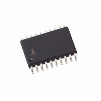
X9221AWS Intersil, X9221AWS Datasheet - Page 10

X9221AWS
Manufacturer Part Number
X9221AWS
Description
IC XDCP DUAL 10K 2-WIRE 20-SOIC
Manufacturer
Intersil
Series
XDCP™r
Datasheet
1.X9221AUSIZT1.pdf
(15 pages)
Specifications of X9221AWS
Taps
64
Resistance (ohms)
10K
Number Of Circuits
2
Temperature Coefficient
30 ppm/°C Typical
Memory Type
Non-Volatile
Interface
I²C, 2-Wire Serial
Voltage - Supply
4.5 V ~ 5.5 V
Operating Temperature
0°C ~ 70°C
Mounting Type
Surface Mount
Package / Case
20-SOIC (7.5mm Width)
Resistance In Ohms
10K
Lead Free Status / RoHS Status
Contains lead / RoHS non-compliant
Available stocks
Company
Part Number
Manufacturer
Quantity
Price
Company:
Part Number:
X9221AWSIZ
Manufacturer:
Intersil
Quantity:
5
Part Number:
X9221AWSZT1
Manufacturer:
INTERSIL
Quantity:
20 000
D.C. OPERATING CHARACTERISTICS (Over recommended operating conditions unless otherwise stated.)
Notes: (1) Absolute Linearity is utilized to determine actual wiper voltage versus expected voltage as determined by wiper position when used as
ENDURANCE AND DATA RETENTION
CAPACITANCE
POWER-UP TIMING
Notes: (5) This parameter is periodically sampled and not 100% tested.
Power Up Requirements (Power up sequencing can affect correct recall of the wiper registers)
The preferred power-on sequence is as follows: First V
reach 90% of its final value before power is applied to the potentiometer pins. The V
be met, and any glitches or slope changes in the V
reverse polarity by more than 0.5V.
Symbol
V
l
I
I
V
Symbol
Symbol
V
t
CC
I
SB
LO
t
C
PUW
OL
t
LI
C
PUR
IH
IL
R
I/O
(2) Relative Linearity is utilized to determine the actual change in voltage between two successive tap positions when used as a potenti-
(3) MI = RTOT/63 or (V
(6) t
IN
V
CC
(5)
(5)
(6)
(6)
a potentiometer.
ometer. It is a measure of the error in step size.
periodically sampled and not 100% tested.
PUR
Supply Current (Active)
V
Input Leakage Current
Output Leakage Current
Input HIGH Voltage
Input LOW Voltage
Output LOW Voltage
CC
Minimum endurance
and t
Data retention
Current (Standby)
Input/output capacitance (SDA)
Input capacitance (A0, A1, A2, A3 and SCL)
Power-up to initiation of read operation
Power-up to initiation of write operation
V
Parameter
PUW
Parameter
CC
Power-up ramp rate
are the delays required from the time V
H
10
/R
H
–V
L
/R
L
)/63, single pot
Parameter
Parameter
Min. Typ.
-1
2
200
Limits
CC
V
Max.
CC
X9221A
CC
100,000
line should be held to <100mV if possible. Also, V
500
0.8
0.4
10
10
3
Min.
100
is stable until the specified operation can be initiated. These parameters are
+ 1
CC
, then the potentiometer pins. It is suggested that V
Unit
mA
µA
µA
µA
V
V
V
f
SCL = SDA = V
V
V
I
SCL
OL
IN
OUT
Max.
= 3mA
= V
Min.
= 100kHz, SDA = Open, Other Inputs = V
0.2
8
6
= V
SS
Data changes per bit per register
SS
to V
to V
CC
CC
Test Conditions
CC
Unit
CC
pF
pF
, Addr. = V
Max.
ramp rate specification should
50
1
5
years
Unit
Test Conditions
SS
V
V
I/O
IN
CC
V/ms
Unit
= 0V
= 0V
ms
ms
should not
August 30, 2006
FN8163.2
SS
CC


