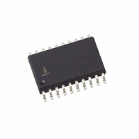
X9221AWS Intersil, X9221AWS Datasheet - Page 4

X9221AWS
Manufacturer Part Number
X9221AWS
Description
IC XDCP DUAL 10K 2-WIRE 20-SOIC
Manufacturer
Intersil
Series
XDCP™r
Datasheet
1.X9221AUSIZT1.pdf
(15 pages)
Specifications of X9221AWS
Taps
64
Resistance (ohms)
10K
Number Of Circuits
2
Temperature Coefficient
30 ppm/°C Typical
Memory Type
Non-Volatile
Interface
I²C, 2-Wire Serial
Voltage - Supply
4.5 V ~ 5.5 V
Operating Temperature
0°C ~ 70°C
Mounting Type
Surface Mount
Package / Case
20-SOIC (7.5mm Width)
Resistance In Ohms
10K
Lead Free Status / RoHS Status
Contains lead / RoHS non-compliant
Available stocks
Company
Part Number
Manufacturer
Quantity
Price
Company:
Part Number:
X9221AWSIZ
Manufacturer:
Intersil
Quantity:
5
Part Number:
X9221AWSZT1
Manufacturer:
INTERSIL
Quantity:
20 000
The next four bits of the slave address are the device
address. The physical device address is defined by
the state of the A0-A3 inputs. The X9221A compares
the serial data stream with the address input state; a
successful compare of all four address bits is required
for the X9221A to respond with an acknowledge.
Acknowledge Polling
The disabling of the inputs, during the internal nonvol-
atile write operation, can be used to take advantage of
the typical 5ms EEPROM write cycle time. Once the
stop condition is issued to indicate the end of the non-
volatile write command the X9221A initiates the inter-
nal write cycle. ACK polling can be initiated
immediately. This involves issuing the start condition
followed by the device slave address. If the X9221A is
still busy with the write operation no ACK will be
returned. If the X9221A has completed the write oper-
ation an ACK will be returned and the master can then
proceed with the next operation.
Flow 1. ACK Polling Sequence
Command Completed
Enter ACK Polling
Nonvolatile Write
Issue Slave
Operation?
Instruction
Returned?
Proceed
Address
Further
START
Issue
Issue
ACK
YES
YES
NO
NO
4
Issue STOP
Issue STOP
Proceed
X9221A
Instruction Structure
The next byte sent to the X9221A contains the instruc-
tion and register pointer information. The four most
significant bits are the instruction. The next four bits
point to one of two pots and when applicable they
point to one of four associated registers. The format is
shown below in Figure 2.
Figure 2. Instruction Byte Format
t
The four high order bits define the instruction. The
sixth bit (P0) selects which one of the two potentiome-
ters is to be affected by the instruction. The last two
bits (R1 and R0) select one of the four registers that is
to be acted upon when a register oriented instruction
is issued.
Four of the nine instructions end with the transmission
of the instruction byte. The basic sequence is illus-
trated in Figure 3. These two-byte instructions
exchange data between the WCR and one of the data
registers. A transfer from a data register to a WCR is
essentially a write to a static RAM. The response of
the wiper to this action will be delayed t
transfer from WCR’s current wiper position to a data
register is a write to nonvolatile memory and takes a
minimum of t
between either potentiometer and their associated
registers or it may occur between both of the potenti-
ometers and one of their associated registers.
Four instructions require a three-byte sequence to
complete. These instructions transfer data between
the host and the X9221A; either between the host and
one of the data registers or directly between the host
and the WCR. These instructions are: Read WCR,
read the current wiper position of the selected pot;
Write WCR, change current wiper position of the
selected pot; Read Data Register, read the contents of
the selected nonvolatile register; Write Data Register,
write a new value to the selected data register. The
sequence of operations is shown in Figure 4.
The Increment/Decrement command is different from
the other commands. Once the command is issued
and the X9221A has responded with an acknowledge,
the master can clock the selected wiper up and/or
down in one segment steps; thereby, providing a fine
I3
Instructions
WR
I2
to complete. The transfer can occur
I1
I0
Potentiometer
0
Select
P0
R1
Register
Select
STPWV
R0
August 30, 2006
FN8163.2
. A


