X9221AWS Intersil, X9221AWS Datasheet - Page 3
X9221AWS
Manufacturer Part Number
X9221AWS
Description
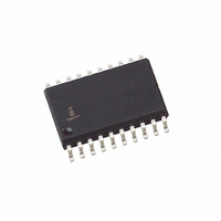
IC XDCP DUAL 10K 2-WIRE 20-SOIC
Manufacturer
Intersil
Series
XDCP™r
Datasheet
1.X9221AUSIZT1.pdf
(15 pages)
Specifications of X9221AWS
Taps
64
Resistance (ohms)
10K
Number Of Circuits
2
Temperature Coefficient
30 ppm/°C Typical
Memory Type
Non-Volatile
Interface
I²C, 2-Wire Serial
Voltage - Supply
4.5 V ~ 5.5 V
Operating Temperature
0°C ~ 70°C
Mounting Type
Surface Mount
Package / Case
20-SOIC (7.5mm Width)
Resistance In Ohms
10K
Lead Free Status / RoHS Status
Contains lead / RoHS non-compliant
Available stocks
Company
Part Number
Manufacturer
Quantity
Price
Company:

Part Number:
X9221AWSIZ
Manufacturer:
Intersil
Quantity:
5
Part Number:
X9221AWSZT1
Manufacturer:
INTERSIL
Quantity:
20 000


PIN NAMES
PRINCIPLES OF OPERATION
The X9221A is a highly integrated microcircuit incor-
porating two resistor arrays, their associated registers
and counters and the serial interface logic providing
direct communication between the host and the XDCP
potentiometers.
Serial Interface
The X9221A supports a bidirectional bus oriented pro-
tocol. The protocol defines any device that sends data
onto the bus as a transmitter and the receiving device
as the receiver. The device controlling the transfer is a
master and the device being controlled is the slave.
The master will always initiate data transfers and pro-
vide the clock for both transmit and receive operations.
Therefore, the X9221A will be considered a slave
device in all applications.
Clock and Data Conventions
Data states on the SDA line can change only during
SCL LOW periods (t
SCL HIGH are reserved for indicating start and stop
conditions.
Start Condition
All commands to the X9221A are preceded by the
start condition, which is a HIGH to LOW transition of
SDA while SCL is HIGH (t
ously monitors the SDA and SCL lines for the start
condition, and will not respond to any command until
this condition is met.
Stop Condition
All communications must be terminated by a stop con-
dition, which is a LOW to HIGH transition of SDA while
SCL is HIGH.
SCL
SDA
A0–A3
V
V
V
RES
H0
L0
W0
/R
/R
/R
H0
H0
Symbol
W0
-V
-V
-V
L1
H1
W1
/R
/R
/R
L0
H1
W1
,
LOW
Serial Clock
Serial Data
Address
Potentiometers
(terminal equivalent)
Potentiometers
(wiper equivalent)
Reserved (Do not connect)
). SDA state changes during
HIGH
3
). The X9221A continu-
Description
X9221A
Acknowledge
Acknowledge is a software convention used to provide
a positive handshake between the master and slave
devices on the bus to indicate the successful receipt of
data. The transmitting device, either the master or the
slave, will release the SDA bus after transmitting eight
bits. The master generates a ninth clock cycle and
during this period the receiver pulls the SDA line LOW
to acknowledge that it successfully received the eight
bits of data. See Figure 7.
The X9221A will respond with an acknowledge after
recognition of a start condition and its slave address
and once again after successful receipt of the com-
mand byte. If the command is followed by a data byte
the X9221A will respond with a final acknowledge.
Array Description
The X9221A is comprised of two resistor arrays. Each
array contains 63 discrete resistive segments that are
connected in series. The physical ends of each array
are equivalent to the fixed terminals of a mechanical
potentiometer (V
At both ends of each array and between each resistor
segment is a FET switch connected to the wiper
(V
switch may be turned on at a time. These switches are
controlled by the Wiper Counter Register (WCR). The
six least significant bits of the WCR are decoded to
select, and enable, one of sixty-four switches.
The WCR may be written directly, or it can be changed
by transferring the contents of one of four associated
data registers into the WCR. These data registers and
the WCR can be read and written by the host system.
Device Addressing
Following a start condition the master must output the
address of the slave it is accessing. The most signifi-
cant four bits of the slave address are the device type
identifier (refer to Figure 1 below). For the X9221A this
is fixed as 0101[B].
Figure 1. Slave Address
W
/R
W
) output. Within each individual array only one
0
Device Type
Identifier
1
H
/R
0
H
and V
1
L
A3
/R
Device Address
L
inputs).
A2
A1
A0
August 30, 2006
FN8163.2
Related parts for X9221AWS
Image
Part Number
Description
Manufacturer
Datasheet
Request
R

Part Number:
Description:
Intersil Corporation [CMOS Serial Controller Interface]
Manufacturer:
Intersil Corporation
Datasheet:
Part Number:
Description:
Manufacturer:
Intersil Corporation
Datasheet:
Part Number:
Description:
357-036-542-201 CARDEDGE 36POS DL .156 BLK LOPRO
Manufacturer:
Intersil Corporation
Datasheet:
Part Number:
Description:
1024-Word x 4-Bit LSI Static RAM
Manufacturer:
Intersil Corporation
Datasheet:
Part Number:
Description:
General Purpose NPN Transistor Arrays FN341.4
Manufacturer:
Intersil Corporation
Datasheet:
Part Number:
Description:
CMOS 16-Bit Microprocessor
Manufacturer:
Intersil Corporation
Datasheet:
Part Number:
Description:
Manufacturer:
Intersil Corporation
Datasheet:
Part Number:
Description:
Manufacturer:
Intersil Corporation
Datasheet:
Part Number:
Description:
Manufacturer:
Intersil Corporation
Datasheet:
Part Number:
Description:
Manufacturer:
Intersil Corporation
Datasheet:
Part Number:
Description:
CMOS 6-Bit Latch and Decoder Memory Interfaces
Manufacturer:
Intersil Corporation
Datasheet:
Part Number:
Description:
CA3046General Purpose NPN Transistor Arrays
Manufacturer:
Intersil Corporation
Datasheet:
Part Number:
Description:
Manufacturer:
Intersil Corporation
Datasheet:
Part Number:
Description:
TR909 DLC/FLC SLIC with Low Power Standby
Manufacturer:
Intersil Corporation
Datasheet:
Part Number:
Description:
Manufacturer:
Intersil Corporation
Datasheet: