ISL22343WFR20Z-TK Intersil, ISL22343WFR20Z-TK Datasheet - Page 14
ISL22343WFR20Z-TK
Manufacturer Part Number
ISL22343WFR20Z-TK
Description
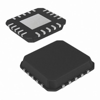
IC POT DGTL 256TP LN LP 20-QFN
Manufacturer
Intersil
Series
XDCP™r
Datasheet
1.ISL22343WFR20Z.pdf
(18 pages)
Specifications of ISL22343WFR20Z-TK
Taps
256
Resistance (ohms)
10K
Number Of Circuits
4
Temperature Coefficient
85 ppm/°C Typical
Memory Type
Non-Volatile
Interface
I²C, 2-Wire Serial
Voltage - Supply
2.25 V ~ 5.5 V
Operating Temperature
-40°C ~ 125°C
Mounting Type
Surface Mount
Package / Case
20-TQFN Exposed Pad
Resistance In Ohms
10K
Lead Free Status / RoHS Status
Lead free / RoHS Compliant
Available stocks
Company
Part Number
Manufacturer
Quantity
Price
Company:

Part Number:
ISL22343WFR20Z-TK
Manufacturer:
SIEMENS
Quantity:
100


SCL is HIGH (see Figure 16). A STOP condition at the end
of a read operation, or at the end of a write operation places
the device in its standby mode.
An ACK (Acknowledge) is a software convention used to
indicate a successful data transfer. The transmitting device,
either master or slave, releases the SDA bus after
transmitting eight bits. During the ninth clock cycle, the
receiver pulls the SDA line LOW to acknowledge the
reception of the eight bits of data (see Figure 17).
The ISL22343 responds with an ACK after recognition of a
START condition followed by a valid Identification Byte, and
once again after successful receipt of an Address Byte. The
ISL22343 also responds with an ACK after receiving a Data
SDA OUTPUT FROM
SDA OUTPUT FROM
TRANSMITTER
SCL FROM
RECEIVER
SDA
SCL
MASTER
SIGNALS FROM
SIGNAL AT SDA
SIGNALS FROM
THE MASTER
THE SLAVE
14
START
FIGURE 16. VALID DATA CHANGES, START AND STOP CONDITIONS
START
FIGURE 17. ACKNOWLEDGE RESPONSE FROM RECEIVER
HIGH IMPEDANCE
S
A
R
T
T
1
FIGURE 18. BYTE WRITE SEQUENCE
IDENTIFICATION
0
1
1
BYTE
0
A2
STABLE
DATA
A1
ISL22343
A0
WRITE
0
A
C
K
CHANGE
DATA
0 0 0 0
ADDRESS
Byte of a write operation. The master must respond with an
ACK after receiving a Data Byte of a read operation
A valid Identification Byte contains 1010 as four MSBs, and
the following three bits matching the logic values present at
pins A2, A1 and A0. The LSB is the Read/Write bit. Its value
is “1” for a Read operation and “0” for a Write operation (See
Table 3).
(MSB)
BYTE
0
1
STABLE
DATA
LOGIC VALUES AT PINS A2, A1 AND A0, RESPECTIVELY
TABLE 3. IDENTIFICATION BYTE FORMAT
0
A
C
K
8
1
DATA
BYTE
0
HIGH IMPEDANCE
STOP
ACK
9
A2
A
C
K
S
T
O
P
A1
A0
March 13, 2008
FN6423.1
(LSB)
R/W
Related parts for ISL22343WFR20Z-TK
Image
Part Number
Description
Manufacturer
Datasheet
Request
R

Part Number:
Description:
Intersil Corporation [CMOS Serial Controller Interface]
Manufacturer:
Intersil Corporation
Datasheet:
Part Number:
Description:
Manufacturer:
Intersil Corporation
Datasheet:
Part Number:
Description:
357-036-542-201 CARDEDGE 36POS DL .156 BLK LOPRO
Manufacturer:
Intersil Corporation
Datasheet:
Part Number:
Description:
1024-Word x 4-Bit LSI Static RAM
Manufacturer:
Intersil Corporation
Datasheet:
Part Number:
Description:
General Purpose NPN Transistor Arrays FN341.4
Manufacturer:
Intersil Corporation
Datasheet:
Part Number:
Description:
CMOS 16-Bit Microprocessor
Manufacturer:
Intersil Corporation
Datasheet:
Part Number:
Description:
Manufacturer:
Intersil Corporation
Datasheet:
Part Number:
Description:
Manufacturer:
Intersil Corporation
Datasheet:
Part Number:
Description:
Manufacturer:
Intersil Corporation
Datasheet:
Part Number:
Description:
Manufacturer:
Intersil Corporation
Datasheet:
Part Number:
Description:
CMOS 6-Bit Latch and Decoder Memory Interfaces
Manufacturer:
Intersil Corporation
Datasheet:
Part Number:
Description:
CA3046General Purpose NPN Transistor Arrays
Manufacturer:
Intersil Corporation
Datasheet:
Part Number:
Description:
Manufacturer:
Intersil Corporation
Datasheet:
Part Number:
Description:
TR909 DLC/FLC SLIC with Low Power Standby
Manufacturer:
Intersil Corporation
Datasheet:
Part Number:
Description:
Manufacturer:
Intersil Corporation
Datasheet: