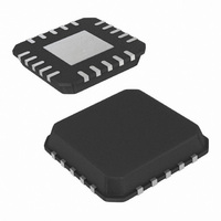
ISL22343WFR20Z-TK Intersil, ISL22343WFR20Z-TK Datasheet - Page 8

ISL22343WFR20Z-TK
Manufacturer Part Number
ISL22343WFR20Z-TK
Description
IC POT DGTL 256TP LN LP 20-QFN
Manufacturer
Intersil
Series
XDCP™r
Datasheet
1.ISL22343WFR20Z.pdf
(18 pages)
Specifications of ISL22343WFR20Z-TK
Taps
256
Resistance (ohms)
10K
Number Of Circuits
4
Temperature Coefficient
85 ppm/°C Typical
Memory Type
Non-Volatile
Interface
I²C, 2-Wire Serial
Voltage - Supply
2.25 V ~ 5.5 V
Operating Temperature
-40°C ~ 125°C
Mounting Type
Surface Mount
Package / Case
20-TQFN Exposed Pad
Resistance In Ohms
10K
Lead Free Status / RoHS Status
Lead free / RoHS Compliant
Available stocks
Company
Part Number
Manufacturer
Quantity
Price
Company:
Part Number:
ISL22343WFR20Z-TK
Manufacturer:
SIEMENS
Quantity:
100
Operating Specifications
NOTES:
10. INL = [V(RW)
12.
13. MI =
14. Roffset = RW
15. RDNL = (RW
16. RINL = [RW
17. R
18.
19. This parameter is not 100% tested.
20. t
21. Parts are 100% tested at +25°C. Temperature limits established by characterization and are not production tested.
11. V
5. Typical values are for T
6. LSB: [V(R
7. ZS error = V(RW)
8. FS error = [V(RW)
9. DNL = [V(RW)
SYMBOL
(Note 19)
(Note 19)
t
t
incremental voltage when changing from one tap to an adjacent tap.
00 hex respectively.
Roffset = RW
volatile write cycle.
TC
TC
SU:A
HD:A
WC
Rpu
Cb
MATCH
MATCH
V
R
is the time from a valid STOP condition at the end of a Write sequence of I
|
RW
=
=
= [V(RWx)i -V(RWy)i]/LSB, for i = 0 to 255, x = 0 to 3, y = 0 to 3.
--------------------------------------------------------------------------------------------- -
[
= [(Rx)i -(Ry)i]/MI, for i = 0 to 255, x = 0 to 3, y = 0 to 3.
--------------------------------------------------------------- -
[
Max V RW
255
Max Ri
W
[
Capacitive Loading of SDA
or SCL
SDA and SCL Bus Pull-up
Resistor Off-chip
A1 and A0 Setup Time
A1 and A0 Hold Time
Max V RW
Max Ri
)
i
255
i
– (MI • i) – RW
i
0
– RW
255
(
– RW
i
(
– i • LSB – V(RW)
/
MI, when measuring between RW and RL.
– V(RW)
(
(
– V(R
(
PARAMETER
/
MI, when measuring between RW and RH.
0
)
255
(
/
0
+
LSB.
) Min Ri
i-1
|
–
/
Min Ri
255. MI is a minimum increment. RW
)
)
– V
W
i
/
A
)
)
MI -1, for i = 16 to 255.
i-1
i
)
+
) Min V RW
0
(
= +25°C and 3.3V supply voltage.
CC
–
]
]
Min V RW
(
/
/
255. V(R
LSB-1, for i = 1 to 255. i is the DCP register setting.
0
)
]
]
/
8
] 2 ⁄
LSB.
/
)
MI, for i = 16 to 255.
(
]
Over the recommended operating conditions unless otherwise specified. (Continued)
(
0
(
×
]/LSB for i = 1 to 255.
+
(
---------------- -
165°C
W
10
)
)
255
Total on-chip and off-chip
Maximum is determined by t
For Cb = 400pF, max is about 2~2.5kΩ
For Cb = 40pF, max is about 15~20kΩ
Before START condition
After STOP condition
i
)
6
)
i
] 2 ⁄
)
and V(R
for i = 16 to 240, T = -40°C to +125°C. Max( ) is the maximum value of the resistance and Min ( ) is
the minimum value of the resistance over the temperature range.
×
+
---------------- -
165°C
10
6
W
)
for i = 16 to 240 decimal, T = -40°C to +125°C. Max( ) is the maximum value of the wiper
0
voltage and Min ( ) is the minimum value of the wiper voltage over the temperature range.
are V(R
TEST CONDITIONS
255
ISL22343
and RW
W
) for the DCP register set to FF hex and 00 hex respectively. LSB is the
R
and t
0
are the measured resistances for the DCP register set to FF hex and
F
2
C serial interface, to the end of the self-timed internal non-
(Note 21)
MIN
600
600
10
1
(Note 5)
TYP
(Note 21)
MAX
400
March 13, 2008
UNIT
FN6423.1
kΩ
pF
ns
ns


