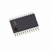
X9409WV24-2.7T1 Intersil, X9409WV24-2.7T1 Datasheet - Page 4

X9409WV24-2.7T1
Manufacturer Part Number
X9409WV24-2.7T1
Description
IC XDCP QUAD 64-TAP 10K 24-TSSOP
Manufacturer
Intersil
Series
XDCP™r
Datasheet
1.X9409WS24ZT1.pdf
(20 pages)
Specifications of X9409WV24-2.7T1
Taps
64
Resistance (ohms)
10K
Number Of Circuits
4
Temperature Coefficient
300 ppm/°C Typical
Memory Type
Non-Volatile
Interface
I²C, 2-Wire Serial
Voltage - Supply
2.7 V ~ 5.5 V
Operating Temperature
0°C ~ 70°C
Mounting Type
Surface Mount
Package / Case
24-TSSOP
Resistance In Ohms
10K
Lead Free Status / RoHS Status
Contains lead / RoHS non-compliant
controlled by the Wiper Counter Register (WCR). The
six bits of the WCR are decoded to select, and enable,
one of sixty-four switches.
The WCR may be written directly, or it can be changed
by transferring the contents of one of four associated
Data Registers into the WCR. These Data Registers
and the WCR can be read and written by the host
system.
Device Addressing
Following a start condition the master must output the
address of the slave it is accessing. The most
significant four bits of the slave address are the device
type identifier (refer to Figure 1 below). For the X9409
this is fixed as 0101[B].
Figure 1. Slave Address
The next four bits of the slave address are the device
address. The physical device address is defined by
the state of the A0 - A3 inputs. The X9409 compares
the serial data stream with the address input state; a
successful compare of all four address bits is required
for the X9409 to respond with an acknowledge. The
A
signals or tied to V
Acknowledge Polling
The disabling of the inputs, during the internal
nonvolatile write operation, can be used to take
advantage of the typical nonvolatile write cycle time.
Once the stop condition is issued to indicate the end of
the nonvolatile write command the X9409 initiates the
internal write cycle. ACK polling can be initiated
immediately. This involves issuing the start condition
followed by the device slave address. If the X9409 is
still busy with the write operation no ACK will be
returned. If the X9409 has completed the write
operation an ACK will be returned and the master can
then proceed with the next operation.
0
- A
3
inputs can be actively driven by CMOS input
0
Device Type
Identifier
1
CC
0
or V
1
SS
4
.
A3
Device Address
A2
A1
A0
X9409
Flow 1. ACK Polling Sequence
Instruction Structure
The next byte sent to the X9409 contains the
instruction and register pointer information. The format
is shown in Figure 2.
Figure 2. Instruction Byte Format
The four high order bits define the instruction. The
next two bits (R1 and R0) select one of the four
registers that is to be acted upon when a register
oriented instruction is issued. The last bits (P1, P0)
select which one of the four potentiometers is to be
affected by the instruction.
Command Completed
Enter ACK Polling
Nonvolatile Write
I3
Issue Slave
Operation?
Instruction
Returned?
Proceed
Address
START
Further
Issue
Issue
Instructions
ACK
I2
YES
YES
I1
NO
I0
NO
Register
R1
Select
R0
Issue STOP
Issue STOP
Pot Select
P1
Proceed
October 12, 2006
P0
FN8192.4


