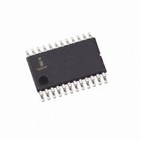
X9409WV24-2.7T1 Intersil, X9409WV24-2.7T1 Datasheet - Page 5

X9409WV24-2.7T1
Manufacturer Part Number
X9409WV24-2.7T1
Description
IC XDCP QUAD 64-TAP 10K 24-TSSOP
Manufacturer
Intersil
Series
XDCP™r
Datasheet
1.X9409WS24ZT1.pdf
(20 pages)
Specifications of X9409WV24-2.7T1
Taps
64
Resistance (ohms)
10K
Number Of Circuits
4
Temperature Coefficient
300 ppm/°C Typical
Memory Type
Non-Volatile
Interface
I²C, 2-Wire Serial
Voltage - Supply
2.7 V ~ 5.5 V
Operating Temperature
0°C ~ 70°C
Mounting Type
Surface Mount
Package / Case
24-TSSOP
Resistance In Ohms
10K
Lead Free Status / RoHS Status
Contains lead / RoHS non-compliant
Four of the nine instructions end with the transmission
of the instruction byte. The basic sequence is
illustrated in Figure 3. These two-byte instructions
exchange data between the Wiper Counter Register
and one of the data registers. A transfer from a Data
Register to a Wiper Counter Register is essentially a
write to a static RAM. The response of the wiper to this
action will be delayed t
Counter Register (current wiper position), to a Data
Register is a write to nonvolatile memory and takes a
minimum of t
between one of the four potentiometers and one of its
associated registers; or it may occur globally, wherein
the transfer occurs between all of the potentiometers
and one of their associated registers.
Four instructions require a three-byte sequence to
complete. These instructions transfer data between
the host and the X9409; either between the host and
one of the data registers or directly between the host
and the Wiper Counter Register. These instructions
are: Read Wiper Counter Register (read the current
Table 1. Instruction Set
Note: (7) 1/0 = data is one or zero
Read Wiper Counter
Register
Write Wiper Counter
Register
Read Data Register
Write Data Register
XFR Data Register to
Wiper Counter Register
XFR Wiper Counter
Register to Data
Register
Global XFR Data
Registers to Wiper
Counter Registers
Global XFR Wiper
Counter Registers to
Data Register
Increment/Decrement
Wiper Counter Register
Instruction
WR
to complete. The transfer can occur
WRL
I
1
1
1
1
1
1
0
1
0
3
5
. A transfer from the Wiper
I
0
0
0
1
1
1
0
0
0
2
I
0
1
1
0
0
1
0
0
1
1
Instruction Set
I
1
0
1
0
1
0
1
0
0
0
R
R
R
R
R
R
R
0
0
0
1
1
1
1
1
1
1
R
R
R
R
R
R
R
0
0
0
0
0
0
0
0
0
0
X9409
P
P
P
P
P
P
P
P
0
0
1
1
1
1
1
1
1
1
wiper position of the selected pot), Write Wiper
Counter Register (change current wiper position of the
selected pot), Read Data Register (read the contents
of the selected nonvolatile register) and Write Data
Register (write a new value to the selected Data
Register). The sequence of operations is shown in
Figure 4.
The Increment/Decrement command is different from
the other commands. Once the command is issued
and the X9409 has responded with an acknowledge,
the master can clock the selected wiper up and/or
down in one segment steps; thereby, providing a fine
tuning capability to the host. For each SCL clock pulse
(t
move one resistor segment towards the V
terminal. Similarly, for each SCL clock pulse while
SDA is LOW, the selected wiper will move one resistor
segment towards the V
illustration of the sequence and timing for this
operation are shown in Figures 5 and 6 respectively.
HIGH
P
P
P
P
P
P
P
P
0
0
0
0
0
0
0
0
0
0
) while SDA is HIGH, the selected wiper will
Read the contents of the Wiper Counter Register
pointed to by P
Write new value to the Wiper Counter Register
pointed to by P
Read the contents of the Data Register pointed to
by P
Write new value to the Data Register pointed to
by P
Transfer the contents of the Data Register
pointed to by P
Wiper Counter Register
Transfer the contents of the Wiper Counter
Register pointed to by P
Register pointed to by R
Transfer the contents of the Data Registers
pointed to by R
respective Wiper Counter Registers
Transfer the contents of both Wiper Counter
Registers to their respective Data Registers
pointed to by R
Enable Increment/decrement of the WCR Latch
pointed to by P
1
1
- P
- P
0
0
and R
and R
1
1
1
1 -
1
1
- P
- P
- P
1
1
- R
- R
P
Operation
- R
- R
0
0
0
0
0
0
L
and R
/R
0
0
of all four pots to their
of all four pots
L
1
1
- P
- R
1
terminal. A detailed
- R
0
0
to the Data
0
to its associated
October 12, 2006
FN8192.4
H
/R
H


