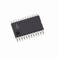
X9409WV24-2.7T1 Intersil, X9409WV24-2.7T1 Datasheet - Page 9

X9409WV24-2.7T1
Manufacturer Part Number
X9409WV24-2.7T1
Description
IC XDCP QUAD 64-TAP 10K 24-TSSOP
Manufacturer
Intersil
Series
XDCP™r
Datasheet
1.X9409WS24ZT1.pdf
(20 pages)
Specifications of X9409WV24-2.7T1
Taps
64
Resistance (ohms)
10K
Number Of Circuits
4
Temperature Coefficient
300 ppm/°C Typical
Memory Type
Non-Volatile
Interface
I²C, 2-Wire Serial
Voltage - Supply
2.7 V ~ 5.5 V
Operating Temperature
0°C ~ 70°C
Mounting Type
Surface Mount
Package / Case
24-TSSOP
Resistance In Ohms
10K
Lead Free Status / RoHS Status
Contains lead / RoHS non-compliant
Instruction Format
Notes: (1) “MACK”/”SACK”: stands for the acknowledge sent by the master/slave.
Read Wiper Counter Register (WCR)
Write Wiper Counter Register (WCR)
Read Data Register (DR)
Write Data Register (DR)
Transfer Data Register (DR) to Wiper Counter Register (WCR)
Write Wiper Counter Register (WCR) to Data Register (DR)
R
R
S
A
R
S
A
R
S
A
R
S
T
A
T
S
T
A
T
S
T
A
R
T
T
T
T
T
T
T
device type
device type
0 1 0 1
0 1 0 1
device type
device type
0 1 0 1
device type
0 1 0 1
device type
0 1 0 1
0 1 0 1
identifier
identifier
identifier
identifier
identifier
identifier
(2) “A3 ~ A0”: stands for the device addresses sent by the master.
(3) “X”: indicates that it is a “0” for testing purpose but physically it is a “don’t care” condition.
(4) “I”: stands for the increment operation, SDA held high during active SCL phase (high).
(5) “D”: stands for the decrement operation, SDA held low during active SCL phase (high).
A
3
A
3
A
addresses
3
A
A
A
addresses
3
3
3
addresses
addresses
addresses
addresses
device
device
device
device
device
device
A
2
A
2
A
2
A
A
A
2
2
2
A
1
A
1
A
A
1
A
A
1
1
1
A
0
A
0
A
0
A
A
A
0
0
0
9
S
A
C
K
C
S
A
K
S
A
C
K
C
C
S
A
C
K
S
A
K
S
A
K
1 1 0 0
1 1 0 1
instruction
instruction
1 1 1 0
1 0 1 1
1 0 0 1 0 0
1 0 1 0 0 0
instruction
instruction
instruction
instruction
opcode
opcode
opcode
opcode
opcode
opcode
DR and WCR
R
1
DR and WCR
R
1
DR and WCR
DR and WCR
R
1
addresses
R
1
addresses
addresses
addresses
addresses
addresses
R
0
R
0
WCR
WCR
R
0
R
0
P
1
P
1
P
1
P
1
P
P
1
1
X9409
P
P
P
0
0
0
P
0
P
0
P
0
S
A
C
K
S
A
C
K
S
A
C
K
S
A
C
K
S
A
C
K
S
A
C
K
(sent by master on SDA)
0 0
0 0
0 0
(sent by master on SDA)
O
S
T
P
(sent by slave on SDA)
O
0 0
S
T
P
(sent by slave on SDA)
wiper position
wiper position
wiper position
HIGH-VOLTAGE
W
P
WRITE CYCLE
W
W
5
P
P
5
5
wiper position
W
P
5
W
P
4
W
W
P
P
4
4
W
P
4
W
P
3
W
W
P
P
3
3
W
P
3
W
P
2
W
W
P
P
2
2
W
P
2
W
P
1
W
W
P
P
1
1
W
P
1
W
P
0
W
W
P
P
0
0
W
P
0
C
S
A
K
M
A
C
K
S
A
C
K
M
A
C
K
O
S
P
T
O
O
S
T
P
S
T
P
O
S
T
P
HIGH-VOLTAGE
WRITE CYCLE
October 12, 2006
FN8192.4


