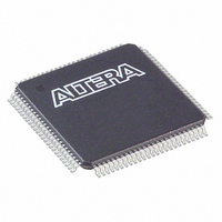
EPM7256AETC100-5N Altera, EPM7256AETC100-5N Datasheet - Page 21

EPM7256AETC100-5N
Manufacturer Part Number
EPM7256AETC100-5N
Description
IC MAX 7000 CPLD 256 100-TQFP
Manufacturer
Altera
Series
MAX® 7000Ar
Datasheet
1.EPM7032AELC44-10N.pdf
(64 pages)
Specifications of EPM7256AETC100-5N
Programmable Type
In System Programmable
Delay Time Tpd(1) Max
5.5ns
Voltage Supply - Internal
3 V ~ 3.6 V
Number Of Logic Elements/blocks
16
Number Of Macrocells
256
Number Of Gates
5000
Number Of I /o
84
Operating Temperature
0°C ~ 70°C
Mounting Type
Surface Mount
Package / Case
100-TQFP, 100-VQFP
Voltage
3.3V
Memory Type
EEPROM
Number Of Logic Elements/cells
16
Family Name
MAX 7000A
# Macrocells
256
Number Of Usable Gates
5000
Frequency (max)
250MHz
Propagation Delay Time
5.5ns
Number Of Logic Blocks/elements
16
# I/os (max)
84
Operating Supply Voltage (typ)
3.3V
In System Programmable
Yes
Operating Supply Voltage (min)
3V
Operating Supply Voltage (max)
3.6V
Operating Temp Range
0C to 70C
Operating Temperature Classification
Commercial
Mounting
Surface Mount
Pin Count
100
Package Type
TQFP
Lead Free Status / RoHS Status
Lead free / RoHS Compliant
Features
-
Lead Free Status / Rohs Status
Compliant
Available stocks
Company
Part Number
Manufacturer
Quantity
Price
Company:
Part Number:
EPM7256AETC100-5N
Manufacturer:
ATERA
Quantity:
1 260
Part Number:
EPM7256AETC100-5N
Manufacturer:
ALTERA/阿尔特拉
Quantity:
20 000
Altera Corporation
SAMPLE/PRELOAD
EXTEST
BYPASS
IDCODE
USERCODE
UESCODE
ISP Instructions
Table 8. MAX 7000A JTAG Instructions
JTAG Instruction
Allows a snapshot of signals at the device pins to be captured and examined during
normal device operation, and permits an initial data pattern output at the device pins
Allows the external circuitry and board-level interconnections to be tested by forcing a
test pattern at the output pins and capturing test results at the input pins
Places the 1-bit bypass register between the TDI and TDO pins, which allows the BST
data to pass synchronously through a selected device to adjacent devices during normal
device operation
Selects the IDCODE register and places it between the TDI and TDO pins, allowing the
IDCODE to be serially shifted out of TDO
Selects the 32-bit USERCODE register and places it between the TDI and TDO pins,
allowing the USERCODE value to be shifted out of TDO. The USERCODE instruction is
available for MAX 7000AE devices only
These instructions select the user electronic signature (UESCODE) and allow the
UESCODE to be shifted out of TDO. UESCODE instructions are available for EPM7128A
and EPM7256A devices only.
These instructions are used when programming MAX 7000A devices via the JTAG ports
with the MasterBlaster, ByteBlasterMV, or BitBlaster download cable, or using a Jam
STAPL File, JBC File, or SVF File via an embedded processor or test equipment.
MAX 7000A Programmable Logic Device Data Sheet
Description
21


