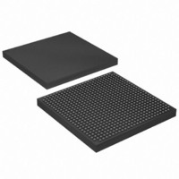
EP1S20F672I7 Altera, EP1S20F672I7 Datasheet - Page 135

EP1S20F672I7
Manufacturer Part Number
EP1S20F672I7
Description
IC STRATIX FPGA 20K LE 672-FBGA
Manufacturer
Altera
Series
Stratix®r
Datasheet
1.EP1S10F780C7.pdf
(276 pages)
Specifications of EP1S20F672I7
Number Of Logic Elements/cells
18460
Number Of Labs/clbs
1846
Total Ram Bits
1669248
Number Of I /o
426
Voltage - Supply
1.425 V ~ 1.575 V
Mounting Type
Surface Mount
Operating Temperature
-40°C ~ 100°C
Package / Case
672-FBGA
Family Name
Stratix
Number Of Logic Blocks/elements
18460
# I/os (max)
426
Frequency (max)
420.17MHz
Process Technology
0.13um (CMOS)
Operating Supply Voltage (typ)
1.5V
Logic Cells
18460
Ram Bits
1669248
Operating Supply Voltage (min)
1.425V
Operating Supply Voltage (max)
1.575V
Operating Temp Range
-40C to 100C
Operating Temperature Classification
Industrial
Mounting
Surface Mount
Pin Count
672
Package Type
FBGA
Lead Free Status / RoHS Status
Contains lead / RoHS non-compliant
Number Of Gates
-
Lead Free Status / Rohs Status
Not Compliant
Available stocks
Company
Part Number
Manufacturer
Quantity
Price
Part Number:
EP1S20F672I7
Manufacturer:
ALTERA/阿尔特拉
Quantity:
20 000
Company:
Part Number:
EP1S20F672I7N
Manufacturer:
ALTERA20
Quantity:
212
Altera Corporation
July 2005
I/O pin has an individual slew-rate control, allowing you to specify the
slew rate on a pin-by-pin basis. The slew-rate control affects both the
rising and falling edges.
Bus Hold
Each Stratix device I/O pin provides an optional bus-hold feature. The
bus-hold circuitry can weakly hold the signal on an I/O pin at its last-
driven state. Since the bus-hold feature holds the last-driven state of the
pin until the next input signal is present, an external pull-up or pull-down
resistor is not needed to hold a signal level when the bus is tri-stated.
Table 2–29
The bus-hold circuitry also pulls undriven pins away from the input
threshold voltage where noise can cause unintended high-frequency
switching. You can select this feature individually for each I/O pin. The
bus-hold output drives no higher than V
signals. If the bus-hold feature is enabled, the programmable pull-up
option cannot be used. Disable the bus-hold feature when using open-
drain outputs with the GTL+ I/O standard or when the I/O pin has been
configured for differential signals.
The bus-hold circuitry uses a resistor with a nominal resistance (R
approximately 7 kΩ to weakly pull the signal level to the last-driven state.
See the DC & Switching Characteristics chapter of the Stratix Device
Handbook, Volume 1 for the specific sustaining current driven through this
resistor and overdrive current used to identify the next-driven input
level. This information is provided for each V
The bus-hold circuitry is active only after configuration. When going into
user mode, the bus-hold circuit captures the value on the pin present at
the end of configuration.
I/O pins
CLK[15..0]
CLK[0,1,2,3,8,9,10,11]
FCLK
FPLL[7..10]CLK
Table 2–29. Bus Hold Support
shows bus hold support for different pin types.
Pin Type
Stratix Device Handbook, Volume 1
CCIO
to prevent overdriving
CCIO
voltage level.
Bus Hold
v
v
Stratix Architecture
BH
2–121
) of


