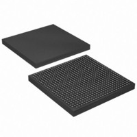
EP1S20F672I7 Altera, EP1S20F672I7 Datasheet - Page 144

EP1S20F672I7
Manufacturer Part Number
EP1S20F672I7
Description
IC STRATIX FPGA 20K LE 672-FBGA
Manufacturer
Altera
Series
Stratix®r
Datasheet
1.EP1S10F780C7.pdf
(276 pages)
Specifications of EP1S20F672I7
Number Of Logic Elements/cells
18460
Number Of Labs/clbs
1846
Total Ram Bits
1669248
Number Of I /o
426
Voltage - Supply
1.425 V ~ 1.575 V
Mounting Type
Surface Mount
Operating Temperature
-40°C ~ 100°C
Package / Case
672-FBGA
Family Name
Stratix
Number Of Logic Blocks/elements
18460
# I/os (max)
426
Frequency (max)
420.17MHz
Process Technology
0.13um (CMOS)
Operating Supply Voltage (typ)
1.5V
Logic Cells
18460
Ram Bits
1669248
Operating Supply Voltage (min)
1.425V
Operating Supply Voltage (max)
1.575V
Operating Temp Range
-40C to 100C
Operating Temperature Classification
Industrial
Mounting
Surface Mount
Pin Count
672
Package Type
FBGA
Lead Free Status / RoHS Status
Contains lead / RoHS non-compliant
Number Of Gates
-
Lead Free Status / Rohs Status
Not Compliant
Available stocks
Company
Part Number
Manufacturer
Quantity
Price
Part Number:
EP1S20F672I7
Manufacturer:
ALTERA/阿尔特拉
Quantity:
20 000
Company:
Part Number:
EP1S20F672I7N
Manufacturer:
ALTERA20
Quantity:
212
High-Speed Differential I/O Support
High-Speed
Differential I/O
Support
2–130
Stratix Device Handbook, Volume 1
Notes to
(1)
(2)
(3)
(4)
(5)
(6)
1.5
1.8
2.5
3.3
Table 2–36. Stratix MultiVolt I/O Support
To drive inputs higher than V
inputs to the device, enable the PCI clamping diode to prevent V
The input pin current may be slightly higher than the typical value.
Although V
different level can still interface with the Stratix device if it has inputs that tolerate the V
Stratix devices can be 5.0-V tolerant with the use of an external resistor and the internal PCI clamp diode.
This is the external signal that is driving the Stratix device.
This represents the system voltage that Stratix supports when a VCCIO pin is connected to a specific voltage level.
For example, when VCCIO is 3.3 V and if the I/O standard is LVTTL/LVCMOS, the output high of the signal
coming out from Stratix is 3.3 V and is compatible with 3.3-V or 5.0-V systems.
V
CCIO
Table
(V)
2–36:
CCIO
f
specifies the voltage necessary for the Stratix device to drive out, a receiving device powered at a
v
1.5 V
v
(2)
The output levels are compatible with systems of the same voltage as the
power supply (i.e., when VCCIO pins are connected to a 1.5-V power
supply, the output levels are compatible with 1.5-V systems). When
VCCIO pins are connected to a 3.3-V power supply, the output high is
3.3 V and is compatible with 3.3-V or 5.0-V systems.
Table 2–36
Stratix devices contain dedicated circuitry for supporting differential
standards at speeds up to 840 Mbps. The following differential I/O
standards are supported in the Stratix device: LVDS, LVPECL,
HyperTransport, and 3.3-V PCML.
There are four dedicated high-speed PLLs in the EP1S10 to EP1S25
devices and eight dedicated high-speed PLLs in the EP1S30 to EP1S80
devices to multiply reference clocks and drive high-speed differential
SERDES channels.
See the Stratix device pin-outs at www.altera.com for additional high
speed DIFFIO pin information for Stratix devices.
1.8 V
v
v
CCIO
Input Signal
but less than 4.1 V, disable the PCI clamping diode. However, to drive 5.0-V
v
v
v
2.5 V
v
summarizes Stratix MultiVolt I/O support.
(2)
(2)
(2)
Note (1)
(5)
v
v
3.3 V
v
v
(2)
(2)
v
5.0 V
(4)
I
from rising above 4.0 V.
v
v
v
1.5 V
v
(3)
(3)
(3)
v
v
1.8 V
v
Output Signal
(3)
(3)
v
2.5 V
v
CCIO
(3)
Altera Corporation
value.
(6)
3.3 V
v
July 2005
5.0 V
v


