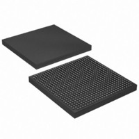
EP1S20F672I7 Altera, EP1S20F672I7 Datasheet - Page 174

EP1S20F672I7
Manufacturer Part Number
EP1S20F672I7
Description
IC STRATIX FPGA 20K LE 672-FBGA
Manufacturer
Altera
Series
Stratix®r
Datasheet
1.EP1S10F780C7.pdf
(276 pages)
Specifications of EP1S20F672I7
Number Of Logic Elements/cells
18460
Number Of Labs/clbs
1846
Total Ram Bits
1669248
Number Of I /o
426
Voltage - Supply
1.425 V ~ 1.575 V
Mounting Type
Surface Mount
Operating Temperature
-40°C ~ 100°C
Package / Case
672-FBGA
Family Name
Stratix
Number Of Logic Blocks/elements
18460
# I/os (max)
426
Frequency (max)
420.17MHz
Process Technology
0.13um (CMOS)
Operating Supply Voltage (typ)
1.5V
Logic Cells
18460
Ram Bits
1669248
Operating Supply Voltage (min)
1.425V
Operating Supply Voltage (max)
1.575V
Operating Temp Range
-40C to 100C
Operating Temperature Classification
Industrial
Mounting
Surface Mount
Pin Count
672
Package Type
FBGA
Lead Free Status / RoHS Status
Contains lead / RoHS non-compliant
Number Of Gates
-
Lead Free Status / Rohs Status
Not Compliant
Available stocks
Company
Part Number
Manufacturer
Quantity
Price
Part Number:
EP1S20F672I7
Manufacturer:
ALTERA/阿尔特拉
Quantity:
20 000
Company:
Part Number:
EP1S20F672I7N
Manufacturer:
ALTERA20
Quantity:
212
Operating Conditions
4–4
Stratix Device Handbook, Volume 1
Notes to
(1)
(2)
(3)
(4)
(5)
(6)
(7)
(8)
(9)
(10) Drive strength is programmable according to the values shown in the Stratix Architecture chapter of the Stratix
V
V
V
V
V
V
V
V
V
V
Table 4–7. 1.8-V I/O Specifications
Table 4–8. 1.5-V I/O Specifications
CCIO
I H
IL
OH
OL
CCIO
I H
IL
OH
OL
Symbol
Symbol
See the Operating Requirements for Altera Devices Data Sheet.
Conditions beyond those listed in
operation at the absolute maximum ratings for extended periods of time may have adverse affects on the device.
Minimum DC input is –0.5 V. During transitions, the inputs may undershoot to –2.0 V for input currents less than
100 mA and periods shorter than 20 ns, or overshoot to the voltage shown in
for input currents less than 100 mA. The overshoot is dependent upon duty cycle of the signal. The DC case is
equivalent to 100% duty cycle.
Maximum V
V
All pins, including dedicated inputs, clock, I/O, and JTAG pins, may be driven before V
powered.
Typical values are for T
This value is specified for normal device operation. The value may vary during power-up. This applies for all
V
Pin pull-up resistance values will lower if an external source drives the pin higher than V
Device Handbook, Volume 1.
CCIO
CCIO
Tables 4–1
maximum and minimum conditions for LVPECL, LVDS, and 3.3-V PCML are shown in parentheses.
settings (3.3, 2.5, 1.8, and 1.5 V).
Output supply voltage
High-level input voltage
Low-level input voltage
High-level output voltage
Low-level output voltage
Output supply voltage
High-level input voltage
Low-level input voltage
High-level output voltage
Low-level output voltage
CC
rise time is 100 ms, and V
through 4–8:
Parameter
Parameter
A
= 25°C, V
Table 4–9. Overshoot Input Voltage with Respect to Duty Cycle (Part 1 of 2)
Table 4–1
CCINT
= 1.5 V, and V
CC
must rise monotonically.
may cause permanent damage to a device. Additionally, device
Vin (V)
4.0
4.1
4.2
I
I
I
I
OH
OL
OH
OL
= 2 to 8 mA
= 2 mA
= –2 to –8 mA
= –2 mA
Conditions
Conditions
CCIO
= 1.5 V, 1.8 V, 2.5 V, and 3.3 V.
(10)
(10)
(10)
(10)
0.65 × V
0.65 × V
0.75 × V
V
Minimum
Minimum
CCIO
Table
1.65
–0.3
–0.3
Maximum Duty Cycle (%)
1.4
– 0.45
4–9, based on input duty cycle
CCIO
CCIO
CCIO
CCINT
0.35 × V
0.35 × V
0.25 × V
CCIO
V
Maximum
Maximum
100
90
50
CCIO
Altera Corporation
1.95
2.25
0.45
.
1.6
and V
+ 0.3
CCIO
CCIO
CCIO
January 2006
CCIO
are
Unit
Unit
V
V
V
V
V
V
V
V
V
V


