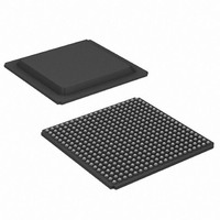
XA3S700A-4FGG400I Xilinx Inc, XA3S700A-4FGG400I Datasheet - Page 14

XA3S700A-4FGG400I
Manufacturer Part Number
XA3S700A-4FGG400I
Description
IC FPGA SPARTAN-3A 700K 400-FBGA
Manufacturer
Xilinx Inc
Series
Spartan™-3A XAr
Datasheet
1.XA3S200A-4FTG256I.pdf
(56 pages)
Specifications of XA3S700A-4FGG400I
Number Of Logic Elements/cells
13248
Number Of Labs/clbs
1472
Total Ram Bits
368640
Number Of I /o
311
Number Of Gates
700000
Voltage - Supply
1.14 V ~ 1.26 V
Mounting Type
Surface Mount
Operating Temperature
-40°C ~ 100°C
Package / Case
400-BGA
Lead Free Status / RoHS Status
Lead free / RoHS Compliant
Available stocks
Company
Part Number
Manufacturer
Quantity
Price
Company:
Part Number:
XA3S700A-4FGG400I
Manufacturer:
XILINX
Quantity:
624
Company:
Part Number:
XA3S700A-4FGG400I
Manufacturer:
Xilinx Inc
Quantity:
10 000
Part Number:
XA3S700A-4FGG400I
Manufacturer:
XILINX/赛灵思
Quantity:
20 000
Differential Output Pairs
Table 14: DC Characteristics of User I/Os Using Differential Signal Standards
14
Notes:
1.
2.
3.
4.
LVDS_25
LVDS_33
BLVDS_25
MINI_LVDS_25
MINI_LVDS_33
RSDS_25
RSDS_33
TMDS_33
PPDS_25
PPDS_33
DIFF_HSTL_I_18
DIFF_HSTL_II_18
DIFF_HSTL_III_18
DIFF_HSTL_I
DIFF_HSTL_III
DIFF_SSTL18_I
DIFF_SSTL18_II
DIFF_SSTL2_I
DIFF_SSTL2_II
DIFF_SSTL3_I
DIFF_SSTL3_II
IOSTANDARD Attribute
The numbers in this table are based on the conditions set forth in
See
Output voltage measurements for all differential standards are made with a termination resistor (R
of the differential signal pair.
At any given time, no more than two of the following differential output standards can be assigned to an I/O bank: LVDS_25,
RSDS_25, MINI_LVDS_25, PPDS_25 when V
V
CCO
"External Termination Requirements for Differential I/O," page
= 3.3V
Min (mV)
Internal
247
247
240
300
300
100
100
400
100
100
GND level
–
–
–
–
–
–
–
–
–
–
–
Logic
V
V
OUTN
OUTP
(mV)
V
Typ
350
350
350
V
OD
–
–
–
–
–
–
–
–
–
–
–
–
–
–
–
–
–
–
Figure 4: Differential Output Voltages
OCM
V
V
V
OD
OH
OL
50%
= Output common mode voltage =
= Output differential voltage =
= Output voltage indicating a Low logic level
= Output voltage indicating a High logic level
CCO
Max (mV)
=2.5V, or LVDS_33, RSDS_33, MINI_LVDS_33, TMDS_33, PPDS_33 when
454
454
460
600
600
400
400
800
400
400
–
–
–
–
–
–
–
–
–
–
–
V
OCM
www.xilinx.com
V
CCO
Min (V)
1.125
1.125
1.0
1.0
1.0
1.0
0.5
0.5
Table 8
– 0.405
–
–
–
–
–
–
–
–
–
–
–
–
V
15.
OUTP
V
V
OD
OUTN
and
V
V
Typ (V)
OUTP
V
Table
OH
1.30
N
OCM
P
0.8
0.8
V
–
–
–
–
–
–
–
–
–
–
–
–
–
–
–
–
–
–
OUTP
- V
13.
OUTN
Differential
I/O Pair Pins
2
+ V
V
DS529-3_11_012907
CCO
V
OUTN
Max (V)
OL
1.375
1.375
1.4
1.4
1.4
1.4
1.4
1.4
–
– 0.190
–
–
–
–
–
–
–
–
–
–
–
T
) of 100Ω across the N and P pins
DS681 (v1.1) February 3, 2009
V
V
V
V
V
V
V
V
V
V
V
TT
TT
CCO
CCO
CCO
CCO
CCO
Min (V)
TT
TT
TT
TT
V
+ 0.475
+ 0.475
Product Specification
+ 0.61
+ 0.81
OH
–
–
–
–
–
–
–
–
–
–
+ 0.6
+ 0.8
– 0.4
– 0.4
– 0.4
– 0.4
– 0.4
V
V
V
V
V
V
TT
TT
Max (V)
TT
TT
TT
TT
V
0.4
0.4
0.4
0.4
0.4
– 0.475
– 0.475
– 0.61
– 0.81
–
–
–
–
–
–
–
–
–
–
OL
– 0.6
– 0.8
R


