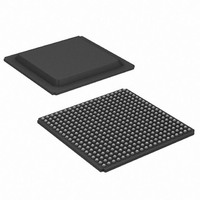
XA3S700A-4FGG400I Xilinx Inc, XA3S700A-4FGG400I Datasheet - Page 28

XA3S700A-4FGG400I
Manufacturer Part Number
XA3S700A-4FGG400I
Description
IC FPGA SPARTAN-3A 700K 400-FBGA
Manufacturer
Xilinx Inc
Series
Spartan™-3A XAr
Datasheet
1.XA3S200A-4FTG256I.pdf
(56 pages)
Specifications of XA3S700A-4FGG400I
Number Of Logic Elements/cells
13248
Number Of Labs/clbs
1472
Total Ram Bits
368640
Number Of I /o
311
Number Of Gates
700000
Voltage - Supply
1.14 V ~ 1.26 V
Mounting Type
Surface Mount
Operating Temperature
-40°C ~ 100°C
Package / Case
400-BGA
Lead Free Status / RoHS Status
Lead free / RoHS Compliant
Available stocks
Company
Part Number
Manufacturer
Quantity
Price
Company:
Part Number:
XA3S700A-4FGG400I
Manufacturer:
XILINX
Quantity:
624
Company:
Part Number:
XA3S700A-4FGG400I
Manufacturer:
Xilinx Inc
Quantity:
10 000
Part Number:
XA3S700A-4FGG400I
Manufacturer:
XILINX/赛灵思
Quantity:
20 000
Table 25:
Timing Measurement Methodology
When measuring timing parameters at the programmable
I/Os, different signal standards call for different test
conditions.
standard.
The method for measuring Input timing is as follows: A
signal that swings between a Low logic level of V
High logic level of V
Some standards also require the application of a bias
voltage to the V
input-switching threshold. The measurement point of the
Input signal (V
and V
The Output test setup is shown in
voltage V
end of which is connected to the Output. For each standard,
R
recommended for minimizing signal reflections. If the
standard does not ordinarily use terminations (for example,
28
Differential Standards
LVDS_25
LVDS_33
BLVDS_25
MINI_LVDS_25
MINI_LVDS_33
LVPECL_25
LVPECL_33
RSDS_25
RSDS_33
TMDS_33
PPDS_25
PPDS_33
DIFF_HSTL_I_18
DIFF_HSTL_II_18
LVCMOS25 with 12mA Drive and
Signal Standard (IOSTANDARD)
Fast Slew Rate to the Following
T
and V
Convert Output Time from
H
.
T
T
is applied to the termination resistor R
Output Timing Adjustments for IOB
generally take on the standard values
Table 26
M
REF
) is commonly located halfway between V
H
pins of a given bank to properly set the
lists the conditions to use for each
is applied to the Input under test.
Speed Grade
Figure
Adjustment
Add the
Below
1.50
0.47
0.11
1.11
0.41
1.73
0.64
0.07
1.28
0.88
0.43
0.41
-4
Input Only
8. A termination
(Continued)
T
L
, the other
Units
and a
ns
ns
ns
ns
ns
ns
ns
ns
ns
ns
ns
ns
www.xilinx.com
L
Table 25:
LVCMOS, LVTTL), then R
open connection, and V
measurement point (V
used at the Output.
Notes:
1.
2.
DIFF_HSTL_III_18
DIFF_HSTL_I
DIFF_HSTL_III
DIFF_SSTL18_I
DIFF_SSTL18_II
DIFF_SSTL2_I
DIFF_SSTL2_II
DIFF_SSTL3_I
DIFF_SSTL3_II
LVCMOS25 with 12mA Drive and
Signal Standard (IOSTANDARD)
Fast Slew Rate to the Following
Convert Output Time from
The numbers in this table are tested using the methodology
presented in
conditions set forth in
These adjustments are used to convert output- and
three-state-path times originally specified for the LVCMOS25
standard with 12 mA drive and Fast slew rate to times that
correspond to other signal standards. Do not adjust times that
measure when outputs go into a high-impedance state.
Notes:
1.
Output Timing Adjustments for IOB
FPGA Output
The names shown in parentheses are
used in the IBIS file.
Figure 8: Output Test Setup
Table 26
M
Table
and are based on the operating
T
) that was used at the Input is also
is set to zero. The same
T
V
is set to 1 MΩ to indicate an
T
8,
(V
Table
DS681 (v1.1) February 3, 2009
REF
R
C
T
L
Speed Grade
(R
Adjustment
)
V
(C
11, and
DS312-3_04_102406
M
Add the
REF
REF
Below
Product Specification
0.36
1.01
1.16
0.49
0.41
0.91
0.11
1.18
0.28
(V
-4
)
MEAS
)
Table
)
(Continued)
13.
Units
ns
ns
ns
ns
ns
ns
ns
ns
ns
R


