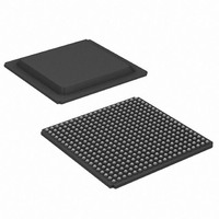
XA3S700A-4FGG400I Xilinx Inc, XA3S700A-4FGG400I Datasheet - Page 18

XA3S700A-4FGG400I
Manufacturer Part Number
XA3S700A-4FGG400I
Description
IC FPGA SPARTAN-3A 700K 400-FBGA
Manufacturer
Xilinx Inc
Series
Spartan™-3A XAr
Datasheet
1.XA3S200A-4FTG256I.pdf
(56 pages)
Specifications of XA3S700A-4FGG400I
Number Of Logic Elements/cells
13248
Number Of Labs/clbs
1472
Total Ram Bits
368640
Number Of I /o
311
Number Of Gates
700000
Voltage - Supply
1.14 V ~ 1.26 V
Mounting Type
Surface Mount
Operating Temperature
-40°C ~ 100°C
Package / Case
400-BGA
Lead Free Status / RoHS Status
Lead free / RoHS Compliant
Available stocks
Company
Part Number
Manufacturer
Quantity
Price
Company:
Part Number:
XA3S700A-4FGG400I
Manufacturer:
XILINX
Quantity:
624
Company:
Part Number:
XA3S700A-4FGG400I
Manufacturer:
Xilinx Inc
Quantity:
10 000
Part Number:
XA3S700A-4FGG400I
Manufacturer:
XILINX/赛灵思
Quantity:
20 000
Pin-to-Pin Setup and Hold Times
Table 19: Pin-to-Pin Setup and Hold Times for the IOB Input Path (System Synchronous)
18
Notes:
1.
2.
3.
4.
Setup Times
Hold Times
The numbers in this table are tested using the methodology presented in
Table 8
This setup time requires adjustment whenever a signal standard other than LVCMOS25 is assigned to the Global Clock Input or the data
Input. If this is true of the Global Clock Input, subtract the appropriate adjustment from
appropriate Input adjustment from the same table.
This hold time requires adjustment whenever a signal standard other than LVCMOS25 is assigned to the Global Clock Input or the data Input.
If this is true of the Global Clock Input, add the appropriate Input adjustment from
appropriate Input adjustment from the same table. When the hold time is negative, it is possible to change the data before the clock’s active
edge.
DCM output jitter is included in all measurements.
Symbol
T
T
T
T
PSDCM
PHDCM
PHFD
PSFD
and
Table
When writing to the Input Flip-Flop (IFF),
the time from the setup of data at the Input
pin to the active transition at a Global Clock
pin. The DCM is in use. No Input Delay is
programmed.
When writing to IFF, the time from the setup
of data at the Input pin to an active transition
at the Global Clock pin. The DCM is not in
use. The Input Delay is programmed.
When writing to IFF, the time from the active
transition at the Global Clock pin to the
point when data must be held at the Input
pin. The DCM is in use. No Input Delay is
programmed.
When writing to IFF, the time from the active
transition at the Global Clock pin to the
point when data must be held at the Input
pin. The DCM is not in use. The Input Delay
is programmed.
11.
Description
www.xilinx.com
LVCMOS25
IFD_DELAY_VALUE = 0,
with DCM
LVCMOS25
IFD_DELAY_VALUE = 5,
without DCM
LVCMOS25
IFD_DELAY_VALUE = 0,
with DCM
LVCMOS25
IFD_DELAY_VALUE = 5,
without DCM
Conditions
Table 26
(4)
(4)
(2)
(2)
(3)
(3)
,
,
,
,
Table
and are based on the operating conditions set forth in
Table
22. If this is true of the data Input, subtract the
22. If this is true of the data Input, add the
XA3S200A
XA3S400A
XA3S700A
XA3S1400A
XA3S200A
XA3S400A
XA3S700A
XA3S1400A
XA3S200A
XA3S400A
XA3S700A
XA3S1400A
XA3S200A
XA3S400A
XA3S700A
XA3S1400A
Device
DS681 (v1.1) February 3, 2009
Speed Grade
Product Specification
-0.52
-0.29
-0.12
-0.56
-0.42
-0.75
-0.69
2.84
2.68
2.57
2.17
2.76
2.60
2.63
2.41
0.00
Min
-4
Units
ns
ns
ns
ns
ns
ns
ns
ns
ns
ns
ns
ns
ns
ns
ns
ns
R


