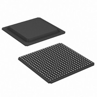
XA3S700A-4FGG400I Xilinx Inc, XA3S700A-4FGG400I Datasheet - Page 50

XA3S700A-4FGG400I
Manufacturer Part Number
XA3S700A-4FGG400I
Description
IC FPGA SPARTAN-3A 700K 400-FBGA
Manufacturer
Xilinx Inc
Series
Spartan™-3A XAr
Datasheet
1.XA3S200A-4FTG256I.pdf
(56 pages)
Specifications of XA3S700A-4FGG400I
Number Of Logic Elements/cells
13248
Number Of Labs/clbs
1472
Total Ram Bits
368640
Number Of I /o
311
Number Of Gates
700000
Voltage - Supply
1.14 V ~ 1.26 V
Mounting Type
Surface Mount
Operating Temperature
-40°C ~ 100°C
Package / Case
400-BGA
Lead Free Status / RoHS Status
Lead free / RoHS Compliant
Available stocks
Company
Part Number
Manufacturer
Quantity
Price
Company:
Part Number:
XA3S700A-4FGG400I
Manufacturer:
XILINX
Quantity:
624
Company:
Part Number:
XA3S700A-4FGG400I
Manufacturer:
Xilinx Inc
Quantity:
10 000
Part Number:
XA3S700A-4FGG400I
Manufacturer:
XILINX/赛灵思
Quantity:
20 000
Serial Peripheral Interface Configuration Timing
Table 51: Timing for SPI Configuration Mode
50
(Open-Drain)
T
T
T
T
T
T
T
PROG_B
CCLK1
CCLKn
MINIT
INITM
CCO
DCC
CCD
PUDC_B
VS[2:0]
CSO_B
Symbol
INIT_B
M[2:0]
CCLK
(Input)
(Input)
(Input)
(Input)
(Input)
MOSI
DIN
Shaded values indicate specifications on attached SPI Flash PROM.
Initial CCLK clock period
CCLK clock period after FPGA loads ConfigRate bitstream option setting
Setup time on VS[2:0] variant-select pins and M[2:0] mode pins before the
rising edge of INIT_B
Hold time on VS[2:0] variant-select pins and M[2:0] mode pins after the
rising edge of INIT_B
MOSI output valid delay after CCLK falling clock edge
Setup time on the DIN data input before CCLK rising clock edge
Hold time on the DIN data input after CCLK rising clock edge
T
MINIT
Pin initially pulled High by internal pull-up resistor if PUDC_B input is Low.
Pin initially high-impedance (Hi-Z) if PUDC_B input is High. External pull-up resistor required on CSO_B.
<1:1:1>
<0:0:1>
PUDC_B must be stable before INIT_B goes High and constant throughout the configuration process.
T
INITM
Figure 13: Waveforms for SPI Configuration
T
CCLK1
Description
T
CSS
Command
Mode input pins M[2:0] and variant select input pins VS[2:0] are sampled when INIT_B
goes High. After this point, input values do not matter until DONE goes High, at which
point these pins become user-I/O pins.
(msb)
T
CCO
www.xilinx.com
T
DSU
T
MCCL1
Command
(msb-1)
T
MCCH1
T
DH
Minimum
Data
50
0
DS681 (v1.1) February 3, 2009
T
T
New ConfigRate active
CCLK1
See
See
See
See
See
MCCL n
Data
T
T
V
Maximum
DCC
Table 45
Table 45
Table 49
Table 49
Table 49
Product Specification
–
–
Data
DS529-3_06_102506
T
T
CCLK n
T
CCD
MCCH n
Units
Data
ns
ns
R


