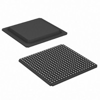
XA3S700A-4FGG400Q Xilinx Inc, XA3S700A-4FGG400Q Datasheet - Page 30

XA3S700A-4FGG400Q
Manufacturer Part Number
XA3S700A-4FGG400Q
Description
IC FPGA SPARTAN-3A 700K 400-FBGA
Manufacturer
Xilinx Inc
Series
Spartan™-3A XAr
Datasheet
1.XA3S200A-4FTG256I.pdf
(56 pages)
Specifications of XA3S700A-4FGG400Q
Number Of Logic Elements/cells
13248
Number Of Labs/clbs
1472
Total Ram Bits
368640
Number Of I /o
311
Number Of Gates
700000
Voltage - Supply
1.14 V ~ 1.26 V
Mounting Type
Surface Mount
Operating Temperature
-40°C ~ 125°C
Package / Case
400-BGA
Lead Free Status / RoHS Status
Lead free / RoHS Compliant
Available stocks
Company
Part Number
Manufacturer
Quantity
Price
Company:
Part Number:
XA3S700A-4FGG400Q
Manufacturer:
XILINX
Quantity:
308
Company:
Part Number:
XA3S700A-4FGG400Q
Manufacturer:
Xilinx Inc
Quantity:
10 000
Part Number:
XA3S700A-4FGG400Q
Manufacturer:
XILINX/赛灵思
Quantity:
20 000
Table 26: Test Methods for Timing Measurement at I/Os (Continued)
The capacitive load (C
and GND. The Output timing for all standards, as published
in the speed files and the data sheet, is always based on a
C
are used for all measurements. Any delay that the test
fixture might contribute to test measurements is subtracted
from those measurements to produce the final timing
numbers as published in the speed files and data sheet.
Using IBIS Models to Simulate Load
Conditions in Application
IBIS models permit the most accurate prediction of timing
delays for a given application. The parameters found in the
IBIS model (V
with the parameters used in
not confuse V
model with V
table. A fourth parameter, C
parameters describe all relevant output test conditions. IBIS
models are found in the Xilinx development software as well
as at the following link:
30
Notes:
1.
2.
3.
DIFF_SSTL18_I
DIFF_SSTL18_II
DIFF_SSTL2_I
DIFF_SSTL2_II
DIFF_SSTL3_I
DIFF_SSTL3_II
L
value of zero. High-impedance probes (less than 1 pF)
http://www.xilinx.com/xlnx/xil_sw_updates_home.jsp
Descriptions of the relevant symbols are as follows:
V
V
V
V
V
R
V
The load capacitance (C
According to the PCI specification.
REF
ICM
M
L
H
T
Signal Standard
T
(IOSTANDARD)
– Low-level test voltage at Input pin
– Effective termination resistance, which takes on a value of 1 MΩ when no parallel termination is required
– Termination voltage
– High-level test voltage at Input pin
– Voltage of measurement point on signal transition
– The common mode input voltage
– The reference voltage for setting the input switching threshold
REF
REF
REF
, R
(the input-switching threshold) from the
(the termination voltage) from the IBIS
REF
L
) is connected between the output
, and V
L
) at the Output pin is 0 pF for all signal standards.
REF
Table 26
V
MEAS
, is always zero. The four
REF
1.25
1.25
0.9
0.9
1.5
1.5
(V)
) correspond directly
(V
T
, R
T
V
V
V
V
V
V
, and V
REF
REF
REF
REF
REF
REF
V
Inputs
L
(V)
– 0.5
– 0.5
– 0.5
– 0.5
– 0.5
– 0.5
M
). Do
www.xilinx.com
V
V
V
V
V
V
REF
REF
REF
REF
REF
REF
V
Delays for a given application are simulated according to its
specific load conditions as follows:
1. Simulate the desired signal standard with the output
2. Record the time to V
3. Simulate the same signal standard with the output
4. Record the time to V
5. Compare the results of steps 2 and 4. Add (or subtract)
H
(V)
+ 0.5
+ 0.5
+ 0.5
+ 0.5
+ 0.5
+ 0.5
driver connected to the test setup shown in
Use parameter values V
C
driver connected to the PCB trace with load. Use the
appropriate IBIS model (including V
and V
load.
the increase (or decrease) in delay to (or from) the
appropriate Output standard adjustment
yield the worst-case delay of the PCB trace.
REF
is zero.
MEAS
R
values) or capacitive value to represent the
T
50
50
50
50
50
50
(Ω)
Outputs
M
MEAS
.
T
, R
.
DS681 (v1.1) February 3, 2009
V
T
1.25
1.25
, and V
T
0.9
0.9
1.5
1.5
(V)
Product Specification
REF
M
from
, R
(Table
Inputs and
REF
Outputs
Table
Figure
V
V
V
V
V
V
V
M
, C
REF
REF
REF
REF
REF
REF
(V)
25) to
REF
26.
8.
,
R


