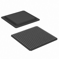
XA3S700A-4FGG400Q Xilinx Inc, XA3S700A-4FGG400Q Datasheet - Page 7

XA3S700A-4FGG400Q
Manufacturer Part Number
XA3S700A-4FGG400Q
Description
IC FPGA SPARTAN-3A 700K 400-FBGA
Manufacturer
Xilinx Inc
Series
Spartan™-3A XAr
Datasheet
1.XA3S200A-4FTG256I.pdf
(56 pages)
Specifications of XA3S700A-4FGG400Q
Number Of Logic Elements/cells
13248
Number Of Labs/clbs
1472
Total Ram Bits
368640
Number Of I /o
311
Number Of Gates
700000
Voltage - Supply
1.14 V ~ 1.26 V
Mounting Type
Surface Mount
Operating Temperature
-40°C ~ 125°C
Package / Case
400-BGA
Lead Free Status / RoHS Status
Lead free / RoHS Compliant
Available stocks
Company
Part Number
Manufacturer
Quantity
Price
Company:
Part Number:
XA3S700A-4FGG400Q
Manufacturer:
XILINX
Quantity:
308
Company:
Part Number:
XA3S700A-4FGG400Q
Manufacturer:
Xilinx Inc
Quantity:
10 000
Part Number:
XA3S700A-4FGG400Q
Manufacturer:
XILINX/赛灵思
Quantity:
20 000
Power Supply Specifications
Table 5: Supply Voltage Thresholds for Power-On Reset
Table 6: Supply Voltage Ramp Rate
Table 7: Supply Voltage Levels Necessary for Preserving CMOS Configuration Latch (CCL) Contents and RAM
Data
DS681 (v1.1) February 3, 2009
Product Specification
Notes:
1.
2.
Notes:
1.
2.
V
NOR Flash, microcontroller) might have specific requirements. Check the data sheet for the attached configuration source. Apply V
for lowest overall power consumption (see
To ensure successful power-on, V
no dips at any point.
V
NOR Flash, microcontroller) might have specific requirements. Check the data sheet for the attached configuration source. Apply V
for lowest overall power consumption (see
To ensure successful power-on, V
no dips at any point.
Symbol
V
V
CCINT
CCINT
DRAUX
V
DRINT
V
V
Symbol
V
Symbol
V
V
CCAUXT
CCAUXR
CCINTR
CCINTT
CCO2T
CCO2R
, V
, V
R
CCAUX
CCAUX
, and V
, and V
V
V
CCINT
CCAUX
Threshold for the V
Threshold for the V
Threshold for the V
Ramp rate from GND to valid V
Ramp rate from GND to valid V
Ramp rate from GND to valid V
CCO
CCO
level required to retain CMOS Configuration Latch (CCL) and RAM data
level required to retain CMOS Configuration Latch (CCL) and RAM data
supplies to the FPGA can be applied in any order. However, the FPGA’s configuration source (SPI Flash, parallel
supplies to the FPGA can be applied in any order. However, the FPGA’s configuration source (SPI Flash, parallel
CCINT
CCINT
, V
, V
CCO
CCO
CCINT
CCAUX
CCO
UG331
UG331
Bank 2, and V
Bank 2, and V
Bank 2 supply
Description
Description
supply
supply
chapter "Powering Spartan-3 Generation FPGAs" for more information).
chapter "Powering Spartan-3 Generation FPGAs" for more information).
CCINT
CCAUX
CCO
Description
www.xilinx.com
Bank 2 supply level
CCAUX
CCAUX
supply level
supply level
supplies must rise through their respective threshold-voltage ranges with
supplies must rise through their respective threshold-voltage ranges with
Min
Min
0.4
0.8
0.8
0.2
0.2
0.2
Max
Max
100
100
100
1.0
2.0
2.0
Min
1.0
2.0
Units
Units
CCINT
CCINT
Units
ms
ms
ms
V
V
V
V
V
last
last
7


