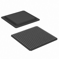
XA3S700A-4FGG400Q Xilinx Inc, XA3S700A-4FGG400Q Datasheet - Page 49

XA3S700A-4FGG400Q
Manufacturer Part Number
XA3S700A-4FGG400Q
Description
IC FPGA SPARTAN-3A 700K 400-FBGA
Manufacturer
Xilinx Inc
Series
Spartan™-3A XAr
Datasheet
1.XA3S200A-4FTG256I.pdf
(56 pages)
Specifications of XA3S700A-4FGG400Q
Number Of Logic Elements/cells
13248
Number Of Labs/clbs
1472
Total Ram Bits
368640
Number Of I /o
311
Number Of Gates
700000
Voltage - Supply
1.14 V ~ 1.26 V
Mounting Type
Surface Mount
Operating Temperature
-40°C ~ 125°C
Package / Case
400-BGA
Lead Free Status / RoHS Status
Lead free / RoHS Compliant
Available stocks
Company
Part Number
Manufacturer
Quantity
Price
Company:
Part Number:
XA3S700A-4FGG400Q
Manufacturer:
XILINX
Quantity:
308
Company:
Part Number:
XA3S700A-4FGG400Q
Manufacturer:
Xilinx Inc
Quantity:
10 000
Part Number:
XA3S700A-4FGG400Q
Manufacturer:
XILINX/赛灵思
Quantity:
20 000
Slave Parallel Mode Timing
Table 50: Timing for the Slave Parallel Configuration Mode
DS681 (v1.1) February 3, 2009
Product Specification
Notes:
1.
2.
(Open-Drain)
Notes:
1.
Setup Times
T
T
T
Hold Times
T
T
T
Clock Timing
T
T
F
SMDCC
SMCSCC
SMCCW
SMCCD
SMCCCS
SMWCC
CCH
CCL
CCPAR
RDWR_B
PROG_B
Symbol
The numbers in this table are based on the operating conditions set forth in
Some Xilinx documents refer to Parallel modes as “SelectMAP” modes.
It is possible to abort configuration by pulling CSI_B Low in a given CCLK cycle, then switching RDWR_B Low or High in any subsequent
cycle for which CSI_B remains Low. The RDWR_B pin asynchronously controls the driver impedance of the D0 - D7 bus. When RDWR_B
switches High, be careful to avoid contention on the D0 - D7 bus.
D0 - D7
(Inputs)
INIT_B
(Input)
CSI_B
(Input)
(Input)
(Input)
CCLK
(2)
R
The time from the setup of data at the D0-D7 pins to the rising transition at the CCLK pin
Setup time on the CSI_B pin before the rising transition at the CCLK pin
Setup time on the RDWR_B pin before the rising transition at the CCLK pin
The time from the rising transition at the CCLK pin to the point when data is last held at
the D0-D7 pins
The time from the rising transition at the CCLK pin to the point when a logic level is last
held at the CSO_B pin
The time from the rising transition at the CCLK pin to the point when a logic level is last
held at the RDWR_B pin
The High pulse width at the CCLK input pin
The Low pulse width at the CCLK input pin
Frequency of the clock signal
at the CCLK input pin
Figure 12: Waveforms for Slave Parallel Configuration
T
SMCCW
T
SMDCC
No bitstream compression
With bitstream compression
Description
Byte 0
T
SMCSCC
www.xilinx.com
T
SMCCD
Byte 1
Table
8.
T
T
MCCH
SCCH
1/F
CCPAR
Byte n
-4 Speed Grade
Min
1.0
15
7
7
0
0
5
5
0
0
T
T
MCCL
SCCL
T
SMCCCS
Byte n+1
Max
80
80
–
–
–
–
–
–
–
–
DS529-3_02_051607
T
SMWCC
Units
MHz
MHz
ns
ns
ns
ns
ns
ns
ns
ns
49


