CS80C286-12 Intersil, CS80C286-12 Datasheet - Page 6
CS80C286-12
Manufacturer Part Number
CS80C286-12
Description
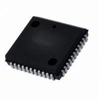
IC CPU 16BIT 5V 12.5MHZ 68-PLCC
Manufacturer
Intersil
Datasheet
1.CS80C286-12.pdf
(60 pages)
Specifications of CS80C286-12
Processor Type
80C286 16-Bit
Speed
12.5MHz
Voltage
5V
Mounting Type
Surface Mount
Package / Case
68-PLCC
Lead Free Status / RoHS Status
Contains lead / RoHS non-compliant
Features
-
Available stocks
Company
Part Number
Manufacturer
Quantity
Price
Company:

Part Number:
CS80C286-12
Manufacturer:
INTERSIL
Quantity:
5 510
Part Number:
CS80C286-12
Manufacturer:
HAR
Quantity:
20 000


Pin Descriptions
NOTES:
Functional Description
Introduction
The Intersil 80C286 microprocessor is a static CMOS ver-
sion of the NMOS 80286 microprocessor. The 80C286 is an
advanced, high-performance microprocessor with specially
optimized capabilities for multiple user and multi-tasking sys-
tems. Depending on the application, the 80C286's perfor-
mance is up to nineteen times faster than the standard
5MHz 8086's, while providing complete upward software
compatibility with Intersil 80C86 and 80C88 CPU family.
The 80C286 operates in two modes: 80C286 real address
mode and protected virtual address mode. Both modes exe-
cute a superset of the 80C86 and 80C88 instruction set.
In 80C286 real address mode programs use real addresses
with up to one megabyte of address space. Programs use vir-
tual addresses in protected virtual address mode, also called
protected mode. In protected mode, the 80C286 CPU automat-
ically maps 1 gigabyte of virtual addresses per task into a 16
megabyte real address space. This mode also provides mem-
ory protection to isolate the operating system and ensure pri-
vacy of each tasks' programs and data. Both modes provide
the same base instruction set, registers and addressing modes.
1. READY is an open-collector signal and should be pulled inactive with an appropriate resistor (620Ω at 10MHz and 12.5MHz, 470Ω at
2. HLDA is only Low if HOLD is inactive (Low).
3. All unused inputs should be pulled to their inactive state with pull up/down resistors.
SYMBOL
RESET
16MHz, 390Ω at 20MHz, 270Ω at 25MHz).
V
V
CC
SS
NUMBER
9, 35, 60
30, 62
PIN
29
The following pin function descriptions are for the 80C286 microprocessor. (Continued)
TYPE
l
l
l
SYSTEM RESET: clears the internal logic of the 80C286 and is active HIGH. The 80C286 may be
reinitialize at any time with a LOW to HIGH transition on RESET which remains active for more than
16 system clock cycles. During RESET active, the output pins of the 80C286 enter the state shown
below.
Operation of the 80C286 begins after a HlGH to LOW transition on RESET. The HIGH to LOW
transition of RESET must be synchronous to the system clock. Approximately 50 system clock
cycles are required by the 80C286 for internal initializations before the first bus cycle to fetch code
from the power-on execution address is performed. A LOW to HIGH transition of RESET
synchronous to the system clock will end a processor cycle at the second HIGH to LOW transition
of the system clock. The LOW to HIGH transition of RESET may be asynchronous to the system
clock; however, in this case it cannot be predetermined which phase of the processor clock will occur
during the next system clock period. Synchronous LOW to HIGH transitions of RESET are required
only for systems where the processor clock must be phase synchronous to another clock.
SYSTEM GROUND: are the ground pins (all must be connected to system ground).
SYSTEM POWER: +5V power supply pins. A 0.1μF capacitor between pins 60 and 62 is recommended.
HIGH IMPEDANCE
PIN VALUE
1 (HIGH)
0 (LOW)
80C286
6
80C286 PIN STATE DURING RESET
The Functional Description describes the following: Static oper-
ation, the base 80C286 architecture common to both modes,
80C286 real address mode, and finally, protected mode.
Static Operation
The 80C286 is comprised of completely static circuitry.
Internal registers, counters, and latches are static and
require no refresh as with dynamic circuit design. This elim-
inates the minimum operating frequency restriction typically
placed on microprocessors. The CMOS 80C286 can oper-
ate from DC to the specified upper frequency limit. The
clock to the processor may be stopped at any point (either
phase one or phase two of the processor clock cycle) and
held there indefinitely. There is, however, a significant
decrease in power requirement if the clock is stopped in
phase two of the processor clock cycle. Details on the clock
relationships will be discussed in the Bus Operation sec-
tion. The ability to stop the clock to the processor is espe-
cially useful for system debug or power critical applications.
S0, S1, PEACK, A
M/IO, COD/lNTA, HLDA (Note 2)
D15 - D0
DESCRIPTION
23
PIN NAMES
- A
0
, BHE, LOCK
Related parts for CS80C286-12
Image
Part Number
Description
Manufacturer
Datasheet
Request
R

Part Number:
Description:
Manufacturer:
TDK Corporation
Datasheet:

Part Number:
Description:
CAP CER 1000PF 250VAC X1Y2 RAD
Manufacturer:
TDK Corporation
Datasheet:

Part Number:
Description:
CAP CER 1000PF 250VAC X1Y2 RAD
Manufacturer:
TDK Corporation
Datasheet:

Part Number:
Description:
Intersil Corporation [CMOS Serial Controller Interface]
Manufacturer:
Intersil Corporation
Datasheet:
Part Number:
Description:
Manufacturer:
Intersil Corporation
Datasheet:
Part Number:
Description:
357-036-542-201 CARDEDGE 36POS DL .156 BLK LOPRO
Manufacturer:
Intersil Corporation
Datasheet:
Part Number:
Description:
1024-Word x 4-Bit LSI Static RAM
Manufacturer:
Intersil Corporation
Datasheet:
Part Number:
Description:
General Purpose NPN Transistor Arrays FN341.4
Manufacturer:
Intersil Corporation
Datasheet:
Part Number:
Description:
CMOS 16-Bit Microprocessor
Manufacturer:
Intersil Corporation
Datasheet:
Part Number:
Description:
Manufacturer:
Intersil Corporation
Datasheet:
Part Number:
Description:
Manufacturer:
Intersil Corporation
Datasheet:
Part Number:
Description:
Manufacturer:
Intersil Corporation
Datasheet:
Part Number:
Description:
Manufacturer:
Intersil Corporation
Datasheet:
Part Number:
Description:
CMOS 6-Bit Latch and Decoder Memory Interfaces
Manufacturer:
Intersil Corporation
Datasheet:
Part Number:
Description:
CA3046General Purpose NPN Transistor Arrays
Manufacturer:
Intersil Corporation
Datasheet: