MC68EC020FG25 Freescale Semiconductor, MC68EC020FG25 Datasheet - Page 103
MC68EC020FG25
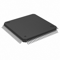
Manufacturer Part Number
MC68EC020FG25
Description
IC MPU 32 BIT 25MHZ 100-QFP
Manufacturer
Freescale Semiconductor
Datasheet
1.MC68EC020AA16.pdf
(306 pages)
Specifications of MC68EC020FG25
Processor Type
M680x0 32-Bit
Speed
25MHz
Voltage
5V
Mounting Type
Surface Mount
Package / Case
100-QFP
Lead Free Status / RoHS Status
Contains lead / RoHS non-compliant
Features
-
Available stocks
Company
Part Number
Manufacturer
Quantity
Price
Company:

Part Number:
MC68EC020FG25
Manufacturer:
FREESCALE
Quantity:
8 831
Company:
Part Number:
MC68EC020FG25
Manufacturer:
Freescale Semiconductor
Quantity:
10 000
Part Number:
MC68EC020FG25
Manufacturer:
MOTOROL
Quantity:
20 000


BERR is recognized during a bus cycle in any of the following cases:
When the processor recognizes a bus error condition, it terminates the current bus cycle
in the normal way. Figure 5-38 shows the timing of a bus error for the case in which
DSACK1/DSACK0 is not asserted. Figure 5-39 shows the timing for a bus error for the
case in which BERR is asserted after DSACK1/DSACK0. Exceptions are taken in both
cases. (Refer to Section 6 Exception Processing for details of bus error exception
processing.) When BERR is asserted during a read cycle that supplies an instruction to
the on-chip cache, the instruction in the cache is marked invalid.
When BERR is asserted after DSACK1/DSACK0, B E R R must be asserted within
parameter #48 (refer to Section 10 Electrical Characteristics) for purely asynchronous
operation, or it must be asserted and remain stable during the sample window, defined by
parameters #27A and #47B, around the next falling edge of the clock after
DSACK1/DSACK0 is recognized. If BERR is not stable at this time, the processor may
exhibit erratic behavior. In this case, data may be present on the bus, but may not be
valid. This sequence may be used by systems that have memory error detection and
correction logic and by external cache memories.
5.5.2 Retry Operation
When BERR and HALT are asserted simultaneously by an external device during a bus
cycle, the processor enters the retry sequence. A delayed retry similar to the delayed
BERR signal described previously can also occur.
The processor terminates the bus cycle, negates the control signals (AS, DS, R/W, SIZ1,
SIZ0, RMC, and, for the MC68020 only, ECS and OCS), and does not begin another bus
cycle until the BERR and HALT signals have been negated by external logic. After a
synchronization delay, the processor retries the previous cycle using the same access
information (address, function code, size, etc.) The BERR signal should be negated before
S2 of the read cycle to ensure correct operation of the retried cycle. Figure 5-40 shows a
late retry operation of a cycle.
The processor retries any read or write cycle of a read-modify-write operation separately;
RMC remains asserted during the entire retry sequence.
Asserting BR along with BERR and HALT provides a relinquish and retry operation. The
MC68020/EC020 does not relinquish the bus during a read-modify-write operation. Any
device that requires the processor to give up the bus and retry a bus cycle during a read-
modify-write cycle must assert BERR and BR only (HALT must not be included). The bus
error handler software should examine the read-modify-write bit in the special status word
(refer to Section 6 Exception Processing) and take the appropriate action to resolve this
type of fault when it occurs.
5-56
1. DSACK1/DSACK0 and HALT are negated and BERR is asserted.
2. HALT and BERR are negated and DSACK1/DSACK0 is asserted. BERR is then
3. BERR and HALT are asserted (see 5.5.2 Retry Operation).
asserted within one clock cycle (HALT remains negated).
M68020 USER’S MANUAL
MOTOROLA
Related parts for MC68EC020FG25
Image
Part Number
Description
Manufacturer
Datasheet
Request
R

Part Number:
Description:
Manufacturer:
Freescale Semiconductor, Inc
Datasheet:
Part Number:
Description:
Manufacturer:
Freescale Semiconductor, Inc
Datasheet:
Part Number:
Description:
Manufacturer:
Freescale Semiconductor, Inc
Datasheet:
Part Number:
Description:
Manufacturer:
Freescale Semiconductor, Inc
Datasheet:
Part Number:
Description:
Manufacturer:
Freescale Semiconductor, Inc
Datasheet:
Part Number:
Description:
Manufacturer:
Freescale Semiconductor, Inc
Datasheet:
Part Number:
Description:
Manufacturer:
Freescale Semiconductor, Inc
Datasheet:
Part Number:
Description:
Manufacturer:
Freescale Semiconductor, Inc
Datasheet:
Part Number:
Description:
Manufacturer:
Freescale Semiconductor, Inc
Datasheet:
Part Number:
Description:
Manufacturer:
Freescale Semiconductor, Inc
Datasheet:
Part Number:
Description:
Manufacturer:
Freescale Semiconductor, Inc
Datasheet:
Part Number:
Description:
Manufacturer:
Freescale Semiconductor, Inc
Datasheet:
Part Number:
Description:
Manufacturer:
Freescale Semiconductor, Inc
Datasheet:
Part Number:
Description:
Manufacturer:
Freescale Semiconductor, Inc
Datasheet:
Part Number:
Description:
Manufacturer:
Freescale Semiconductor, Inc
Datasheet: