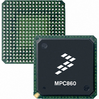
MC68MH360ZP25VL Freescale Semiconductor, MC68MH360ZP25VL Datasheet - Page 141

MC68MH360ZP25VL
Manufacturer Part Number
MC68MH360ZP25VL
Description
IC MPU QUICC ETHER 25MHZ 357PBGA
Manufacturer
Freescale Semiconductor
Datasheet
1.MC68MH360VR25LR2.pdf
(158 pages)
Specifications of MC68MH360ZP25VL
Processor Type
M683xx 32-Bit
Speed
25MHz
Voltage
3.3V
Mounting Type
Surface Mount
Package / Case
357-PBGA
Lead Free Status / RoHS Status
Contains lead / RoHS non-compliant
Features
-
Available stocks
Company
Part Number
Manufacturer
Quantity
Price
Company:
Part Number:
MC68MH360ZP25VL
Manufacturer:
Freescale Semiconductor
Quantity:
10 000
- Current page: 141 of 158
- Download datasheet (5Mb)
However, this configuration works only if the single master S/T or U interface is guaranteed
to be active, constantly generating synchronized DCL and FSC signals for the network.
Since the designated master transceiver cannot be guaranteed active, all transceivers must
be configured in slave mode, and the problem of synchronization remains.
DCL and FSC must be generated from within the network and cannot be derived from an
independent source (e.g., crystal or oscillator). However, the S/T and U interfaces, even in
slave mode, provide a way to generate these signals as explained in the following sections.
C.3.1 MC145574 S/T Interface
To facilitate the generation of timing signals required by the slave IDL interface, TCLK is
provided in the S/T interface. The TCLK signal will output a clock synchronized to the
received data transmitted by the NT. That clock is output only when the S/T interface is
active and when the DCL and FSC signals are present (both conditions are required
simultaneously). This TCLK signal can be used to provide network timing. Its frequency is
selectable via the SCP.
The TCLK signal of the MC145574 is enabled by setting OR7[5]. BR13[5] and BR7[2]
determine the TCLK frequency as shown in Table C-1.
A TCLK signal configured as a 2.048-MHz clock can be used as the DCL for the IDL bus.
Dividing the TCLK signal by 256 provides the 8-KHz frame sync FSC. Since the FSC must
have a pulse between one DCL and eight DCLs in width, additional logic may be needed
after the divider to generate a signal with a correct duty cycle.
Figure C-4 and Figure C-5 show a schematic and a timing diagram, respectively, for a logic
design used to generate a 8-KHz FSC with a 1-DCL width pulse from a 2.048-MHz clock
(TCLK).
Table C-1. TCLK Frequencies Selected by BR13[5] and BR7[2]
Appendix C. Connecting ISDN Multiple S/T or U Interfaces to QUICC32
Freescale Semiconductor, Inc.
For More Information On This Product,
BR13[5]
0
0
1
1
Go to: www.freescale.com
BR7[2]
0
1
0
1
2.56 MHz
2.048 MHz
1.536 MHz
512 KHz
TCLK
Related parts for MC68MH360ZP25VL
Image
Part Number
Description
Manufacturer
Datasheet
Request
R
Part Number:
Description:
Manufacturer:
Freescale Semiconductor, Inc
Datasheet:
Part Number:
Description:
Manufacturer:
Freescale Semiconductor, Inc
Datasheet:
Part Number:
Description:
Manufacturer:
Freescale Semiconductor, Inc
Datasheet:
Part Number:
Description:
Manufacturer:
Freescale Semiconductor, Inc
Datasheet:
Part Number:
Description:
Manufacturer:
Freescale Semiconductor, Inc
Datasheet:
Part Number:
Description:
Manufacturer:
Freescale Semiconductor, Inc
Datasheet:
Part Number:
Description:
Manufacturer:
Freescale Semiconductor, Inc
Datasheet:
Part Number:
Description:
Manufacturer:
Freescale Semiconductor, Inc
Datasheet:
Part Number:
Description:
Manufacturer:
Freescale Semiconductor, Inc
Datasheet:
Part Number:
Description:
Manufacturer:
Freescale Semiconductor, Inc
Datasheet:
Part Number:
Description:
Manufacturer:
Freescale Semiconductor, Inc
Datasheet:
Part Number:
Description:
Manufacturer:
Freescale Semiconductor, Inc
Datasheet:
Part Number:
Description:
Manufacturer:
Freescale Semiconductor, Inc
Datasheet:
Part Number:
Description:
Manufacturer:
Freescale Semiconductor, Inc
Datasheet:
Part Number:
Description:
Manufacturer:
Freescale Semiconductor, Inc
Datasheet:


