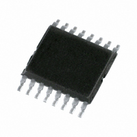
SC18IS602BIPW,112 NXP Semiconductors, SC18IS602BIPW,112 Datasheet - Page 10

SC18IS602BIPW,112
Manufacturer Part Number
SC18IS602BIPW,112
Description
IC BRIDGE SPI/I2C 16-TSSOP
Manufacturer
NXP Semiconductors
Specifications of SC18IS602BIPW,112
Controller Type
I²C Bus Controller
Interface
I²C
Voltage - Supply
2.4 V ~ 3.6 V
Current - Supply
11mA
Operating Temperature
-40°C ~ 85°C
Mounting Type
Surface Mount
Package / Case
16-TSSOP
Operating Temperature Classification
Military
Operating Temperature (max)
125C
Package Type
TSSOP
Rad Hardened
No
Maximum Operating Frequency
4.5 MHz
Maximum Operating Temperature
+ 125 C
Minimum Operating Temperature
- 55 C
Mounting Style
SMD/SMT
Supply Voltage (max)
3.6 V
Supply Voltage (min)
2.4 V
For Use With
568-4705 - DEMO BOARD I2C TO SPI SC18IS602
Lead Free Status / RoHS Status
Lead free / RoHS Compliant
Other names
568-4785-5
935286182112
SC18IS602BIPW
SC18IS602BIPW,112
SC18IS602BIPW
935286182112
SC18IS602BIPW
SC18IS602BIPW,112
SC18IS602BIPW
Available stocks
Company
Part Number
Manufacturer
Quantity
Price
Company:
Part Number:
SC18IS602BIPW,112
Manufacturer:
NXP
Quantity:
463
NXP Semiconductors
SC18IS602B
Product data sheet
7.1.11.1 Quasi-bidirectional output configuration
7.1.11 GPIO Configuration - Function ID F7h
The pins defined as GPIO may be configured by software to one of four types on a
pin-by-pin basis. These are: quasi-bidirectional, push-pull, open-drain, and input-only.
Two bits select the output type for each port pin.
Table 9.
Table 10.
The SSn pins defined as GPIO, for example SS0.0 and SS0.1, may be configured by
software to one of four types. These are: quasi-bidirectional, push-pull, open-drain, and
input-only. Two configuration bits in GPIO Configuration register for each pin select the
type for each pin. A pin has Schmitt-triggered input that also has a glitch suppression
circuit.
Quasi-bidirectional outputs can be used both as an input and output without the need to
reconfigure the pin. This is possible because when the pin outputs a logic HIGH, it is
weakly driven, allowing an external device to pull the pin LOW. When the pin is driven
LOW, it is driven strongly and able to sink a large current. There are three pull-up
transistors in the quasi-bidirectional output that serve different purposes.
One of these pull-ups, called the ‘very weak’ pull-up, is turned on whenever the port latch
for the pin contains a logic 1. This very weak pull-up sources a very small current that will
pull the pin HIGH if it is left floating.
A second pull-up, called the ‘weak’ pull-up, is turned on when the port latch for the pin
contains a logic 1 and the pin itself is also at a logic 1 level. This pull-up provides the
primary source current for a quasi-bidirectional pin that is outputting a 1. If this pin is
Bit
7
6
5
4
3
2
1
0
SS3.1
7
Symbol
SS3.1
SS3.0
SS2.1
SS2.0
SS1.1
SS1.0
SS0.1
SS0.0
GPIO Configuration (F7h) bit allocation
GPIO Configuration (F7h) bit description
SS3.0
All information provided in this document is subject to legal disclaimers.
6
Description
Rev. 5 — 3 August 2010
SS2.1
SS3[1:0] = 00: quasi-bidirectional
SS3[1:0] = 01: push-pull
SS3[1:0] = 10: input-only (high-impedance)
SS3[1:0] = 11: open-drain
SS2[1:0] = 00: quasi-bidirectional
SS2[1:0] = 01: push-pull
SS2[1:0] = 10: input-only (high-impedance)
SS2[1:0] = 11: open-drain
SS1[1:0] = 00: quasi-bidirectional
SS1[1:0] = 01: push-pull
SS1[1:0] = 10: input-only (high-impedance)
SS1[1:0] = 11: open-drain
SS0[1:0] = 00: quasi-bidirectional
SS0[1:0] = 01: push-pull
SS0[1:0] = 10: input-only (high-impedance)
SS0[1:0] = 11: open-drain
5
SS2.0
4
SS1.1
3
SS1.0
2
SC18IS602B
I
2
C-bus to SPI bridge
SS0.1
© NXP B.V. 2010. All rights reserved.
1
SS0.0
10 of 25
0


