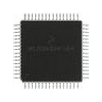
MC68HC908LD60IFU Freescale Semiconductor, MC68HC908LD60IFU Datasheet - Page 100

MC68HC908LD60IFU
Manufacturer Part Number
MC68HC908LD60IFU
Description
Manufacturer
Freescale Semiconductor
Datasheet
1.MC68HC908LD60IFU.pdf
(292 pages)
Specifications of MC68HC908LD60IFU
Cpu Family
HC08
Device Core Size
8b
Frequency (max)
6MHz
Program Memory Type
Flash
Program Memory Size
60KB
Total Internal Ram Size
1KB
# I/os (max)
39
Number Of Timers - General Purpose
2
Operating Supply Voltage (typ)
3.3V
Operating Supply Voltage (max)
3.6V
Operating Supply Voltage (min)
3V
On-chip Adc
6-chx8-bit
Instruction Set Architecture
CISC
Operating Temp Range
0C to 85C
Operating Temperature Classification
Commercial
Mounting
Surface Mount
Pin Count
64
Package Type
PQFP
Lead Free Status / Rohs Status
Compliant
Available stocks
Company
Part Number
Manufacturer
Quantity
Price
- Current page: 100 of 292
- Download datasheet (4Mb)
Clock Generator Module (CGM)
8.6.2 PLL Bandwidth Control Register (PBWC)
Technical Data
100
NOTE:
PLLON — PLL On Bit
BCS — Base Clock Select Bit
PLLON and BCS have built-in protection that prevents the base clock
selector circuit from selecting the VCO clock as the source of the base
clock if the PLL is off. Therefore, PLLON cannot be cleared when BCS
is set, and BCS cannot be set when PLLON is clear. If the PLL is off
(PLLON = 0), selecting CGMVCLK requires two writes to the PLL control
register.
The PLL bandwidth control register does the following:
This read/write bit activates the PLL and enables the VCO clock,
CGMVCLK. PLLON cannot be cleared if the VCO clock is driving the
base clock, DCLK1 (BCS = 1). Reset sets this bit so that the loop can
stabilize as the MCU is powering up.
This read/write bit selects either the crystal oscillator output,
OSCXCLK, or the VCO clock, CGMVCLK, as the source of the CGM
output, DCLK1. BCS cannot be set while the PLLON bit is clear. After
toggling BCS, it may take up to three OSCXCLK and three CGMVCLK
cycles to complete the transition from one source clock to the other.
During the transition, DCLK1 is held in stasis. Reset and the STOP
instruction clear the BCS bit.
•
•
•
•
1 = PLL on
0 = PLL off
1 = DCLK1 driven by CGMVCLK
0 = DCLK1 driven by OSCXCLK
Selects automatic or manual (software-controlled) bandwidth
control mode
Indicates when the PLL is locked
In automatic bandwidth control mode, indicates when the PLL is in
acquisition or tracking mode
In manual operation, forces the PLL into acquisition or tracking
mode
Clock Generator Module (CGM)
MC68HC908LD60
Freescale Semiconductor
—
Rev. 1.1
Related parts for MC68HC908LD60IFU
Image
Part Number
Description
Manufacturer
Datasheet
Request
R
Part Number:
Description:
Manufacturer:
Freescale Semiconductor, Inc
Datasheet:
Part Number:
Description:
Manufacturer:
Freescale Semiconductor, Inc
Datasheet:
Part Number:
Description:
Manufacturer:
Freescale Semiconductor, Inc
Datasheet:
Part Number:
Description:
Manufacturer:
Freescale Semiconductor, Inc
Datasheet:
Part Number:
Description:
Manufacturer:
Freescale Semiconductor, Inc
Datasheet:
Part Number:
Description:
Manufacturer:
Freescale Semiconductor, Inc
Datasheet:
Part Number:
Description:
Manufacturer:
Freescale Semiconductor, Inc
Datasheet:
Part Number:
Description:
Manufacturer:
Freescale Semiconductor, Inc
Datasheet:
Part Number:
Description:
Manufacturer:
Freescale Semiconductor, Inc
Datasheet:
Part Number:
Description:
Manufacturer:
Freescale Semiconductor, Inc
Datasheet:
Part Number:
Description:
Manufacturer:
Freescale Semiconductor, Inc
Datasheet:
Part Number:
Description:
Manufacturer:
Freescale Semiconductor, Inc
Datasheet:
Part Number:
Description:
Manufacturer:
Freescale Semiconductor, Inc
Datasheet:
Part Number:
Description:
Manufacturer:
Freescale Semiconductor, Inc
Datasheet:
Part Number:
Description:
Manufacturer:
Freescale Semiconductor, Inc
Datasheet:


