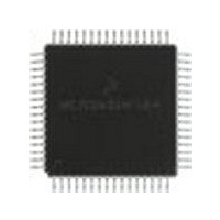
MC68HC908LD60IFU Freescale Semiconductor, MC68HC908LD60IFU Datasheet - Page 154

MC68HC908LD60IFU
Manufacturer Part Number
MC68HC908LD60IFU
Description
Manufacturer
Freescale Semiconductor
Datasheet
1.MC68HC908LD60IFU.pdf
(292 pages)
Specifications of MC68HC908LD60IFU
Cpu Family
HC08
Device Core Size
8b
Frequency (max)
6MHz
Program Memory Type
Flash
Program Memory Size
60KB
Total Internal Ram Size
1KB
# I/os (max)
39
Number Of Timers - General Purpose
2
Operating Supply Voltage (typ)
3.3V
Operating Supply Voltage (max)
3.6V
Operating Supply Voltage (min)
3V
On-chip Adc
6-chx8-bit
Instruction Set Architecture
CISC
Operating Temp Range
0C to 85C
Operating Temperature Classification
Commercial
Mounting
Surface Mount
Pin Count
64
Package Type
PQFP
Lead Free Status / Rohs Status
Compliant
Available stocks
Company
Part Number
Manufacturer
Quantity
Price
- Current page: 154 of 292
- Download datasheet (4Mb)
Timer Interface Module (TIM)
11.7.2 Stop Mode
11.8 TIM During Break Interrupts
11.9 I/O Signals
Technical Data
154
If TIM functions are not required during wait mode, reduce power
consumption by stopping the TIM before executing the WAIT instruction.
The TIM is inactive after the execution of a STOP instruction. The STOP
instruction does not affect register conditions or the state of the TIM
counter. TIM operation resumes when the MCU exit stop mode after an
external interrupt.
A break interrupt stops the TIM counter.
The system integration module (SIM) controls whether status bits in
other modules can be cleared during the break state. The BCFE bit in
the break flag control register (BFCR) enables software to clear status
bits during the break state. (See
Register.)
To allow software to clear status bits during a break interrupt, write a
logic one to the BCFE bit. If a status bit is cleared during the break state,
it remains cleared when the MCU exits the break state.
To protect status bits during the break state, write a logic zero to the
BCFE bit. With BCFE at logic zero (its default state), software can read
and write I/O registers during the break state without affecting status
bits. Some status bits have a two-step read/write clearing procedure. If
software does the first step on such a bit before the break, the bit cannot
change during the break state as long as BCFE is at logic zero. After the
break, doing the second step clears the status bit.
The TIM channel I/O pin is CLAMP/TCH0. The pin is shared with sync
processor CLAMP output signal.
TCH0 pin is programmable independently as an input capture pin or an
output compare pin. It also can be configured as a buffered output
compare or buffered PWM pin.
Timer Interface Module (TIM)
21.6.4 SIM Break Flag Control
MC68HC908LD60
Freescale Semiconductor
—
Rev. 1.1
Related parts for MC68HC908LD60IFU
Image
Part Number
Description
Manufacturer
Datasheet
Request
R
Part Number:
Description:
Manufacturer:
Freescale Semiconductor, Inc
Datasheet:
Part Number:
Description:
Manufacturer:
Freescale Semiconductor, Inc
Datasheet:
Part Number:
Description:
Manufacturer:
Freescale Semiconductor, Inc
Datasheet:
Part Number:
Description:
Manufacturer:
Freescale Semiconductor, Inc
Datasheet:
Part Number:
Description:
Manufacturer:
Freescale Semiconductor, Inc
Datasheet:
Part Number:
Description:
Manufacturer:
Freescale Semiconductor, Inc
Datasheet:
Part Number:
Description:
Manufacturer:
Freescale Semiconductor, Inc
Datasheet:
Part Number:
Description:
Manufacturer:
Freescale Semiconductor, Inc
Datasheet:
Part Number:
Description:
Manufacturer:
Freescale Semiconductor, Inc
Datasheet:
Part Number:
Description:
Manufacturer:
Freescale Semiconductor, Inc
Datasheet:
Part Number:
Description:
Manufacturer:
Freescale Semiconductor, Inc
Datasheet:
Part Number:
Description:
Manufacturer:
Freescale Semiconductor, Inc
Datasheet:
Part Number:
Description:
Manufacturer:
Freescale Semiconductor, Inc
Datasheet:
Part Number:
Description:
Manufacturer:
Freescale Semiconductor, Inc
Datasheet:
Part Number:
Description:
Manufacturer:
Freescale Semiconductor, Inc
Datasheet:


