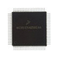
MC68HC912B32VFU8 Freescale Semiconductor, MC68HC912B32VFU8 Datasheet - Page 208

MC68HC912B32VFU8
Manufacturer Part Number
MC68HC912B32VFU8
Description
Manufacturer
Freescale Semiconductor
Datasheet
1.MC68HC912B32VFU8.pdf
(334 pages)
Specifications of MC68HC912B32VFU8
Cpu Family
HC12
Device Core Size
16b
Frequency (max)
8MHz
Interface Type
SCI/SPI
Program Memory Type
EPROM
Program Memory Size
32KB
Total Internal Ram Size
1KB
# I/os (max)
63
Operating Supply Voltage (typ)
5V
Operating Supply Voltage (max)
5.5V
Operating Supply Voltage (min)
4.5V
On-chip Adc
8-chx10-bit
Instruction Set Architecture
CISC
Operating Temp Range
-40C to 105C
Operating Temperature Classification
Industrial
Mounting
Surface Mount
Pin Count
80
Package Type
PQFP
Lead Free Status / Rohs Status
Not Compliant
Available stocks
Company
Part Number
Manufacturer
Quantity
Price
Part Number:
MC68HC912B32VFU8
Manufacturer:
MOTOROLA/摩托罗拉
Quantity:
20 000
- Current page: 208 of 334
- Download datasheet (2Mb)
Serial Interface
form a distributed 16-bit register. When a data transfer operation is performed, this 16-bit register is
serially shifted eight bit positions by the SCK clock from the master so the data is exchanged effectively
between the master and the slave.
14.4 Port S
In all modes, port S bits PS7–PS0 can be used for either general-purpose I/O or with the SCI and SPI
subsystems. During reset, port S pins are configured as high-impedance inputs (DDRS is cleared).
14.4.1 Port S Data Register
Read: Anytime; inputs return pin level; outputs return pin driver input level
Write: Data stored in internal latch; drives pins only if configured for output; does
Port S shares function with the on-chip serial systems, SPI0 and SCI0.
14.4.2 Port S Data Direction Register
Read: Anytime
Write: Anytime
After reset, all general-purpose I/O are configured for input only.
208
0 = Configure the corresponding I/O pin for input only.
1 = Configure the corresponding I/O pin for output.
not change pin state when pin configured for SPI or SCI output
Pin Function
Address:
Address:
Some slave devices are simple and either accept data from the master
without returning data to the master or pass data to the master without
requiring data from the master.
Reset:
Read:
Write:
Reset:
Read:
Write:
$00D7
DDS7
Bit 7
$00D6
Bit 7
0
PS7
Figure 14-21. Port S Data Direction Register (DDRS)
SS
CS
Figure 14-20. Port S Data Register (PORTS)
DDS6
SCK
6
0
PS6
6
M68HC12B Family Data Sheet, Rev. 9.1
After reset all bits configured as general-purpose inputs
DDS5
MOMI
MOSI
5
0
PS5
5
NOTE
DDS4
MISO
SISO
4
0
PS4
4
DDS3
3
0
PS3
—
3
DDS2
2
0
PS2
—
2
DDS1
TXD0
1
0
PS1
1
Freescale Semiconductor
DDS0
Bit 0
RXD0
Bit 0
0
PS0
Related parts for MC68HC912B32VFU8
Image
Part Number
Description
Manufacturer
Datasheet
Request
R
Part Number:
Description:
Manufacturer:
Freescale Semiconductor, Inc
Datasheet:
Part Number:
Description:
Manufacturer:
Freescale Semiconductor, Inc
Datasheet:
Part Number:
Description:
Manufacturer:
Freescale Semiconductor, Inc
Datasheet:
Part Number:
Description:
Manufacturer:
Freescale Semiconductor, Inc
Datasheet:
Part Number:
Description:
Manufacturer:
Freescale Semiconductor, Inc
Datasheet:
Part Number:
Description:
Manufacturer:
Freescale Semiconductor, Inc
Datasheet:
Part Number:
Description:
Manufacturer:
Freescale Semiconductor, Inc
Datasheet:
Part Number:
Description:
Manufacturer:
Freescale Semiconductor, Inc
Datasheet:
Part Number:
Description:
Manufacturer:
Freescale Semiconductor, Inc
Datasheet:
Part Number:
Description:
Manufacturer:
Freescale Semiconductor, Inc
Datasheet:
Part Number:
Description:
Manufacturer:
Freescale Semiconductor, Inc
Datasheet:
Part Number:
Description:
Manufacturer:
Freescale Semiconductor, Inc
Datasheet:
Part Number:
Description:
Manufacturer:
Freescale Semiconductor, Inc
Datasheet:
Part Number:
Description:
Manufacturer:
Freescale Semiconductor, Inc
Datasheet:
Part Number:
Description:
Manufacturer:
Freescale Semiconductor, Inc
Datasheet:


