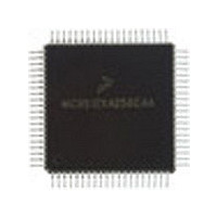
MC68HC912B32VFU8 Freescale Semiconductor, MC68HC912B32VFU8 Datasheet - Page 99

MC68HC912B32VFU8
Manufacturer Part Number
MC68HC912B32VFU8
Description
Manufacturer
Freescale Semiconductor
Datasheet
1.MC68HC912B32VFU8.pdf
(334 pages)
Specifications of MC68HC912B32VFU8
Cpu Family
HC12
Device Core Size
16b
Frequency (max)
8MHz
Interface Type
SCI/SPI
Program Memory Type
EPROM
Program Memory Size
32KB
Total Internal Ram Size
1KB
# I/os (max)
63
Operating Supply Voltage (typ)
5V
Operating Supply Voltage (max)
5.5V
Operating Supply Voltage (min)
4.5V
On-chip Adc
8-chx10-bit
Instruction Set Architecture
CISC
Operating Temp Range
-40C to 105C
Operating Temperature Classification
Industrial
Mounting
Surface Mount
Pin Count
80
Package Type
PQFP
Lead Free Status / Rohs Status
Not Compliant
Available stocks
Company
Part Number
Manufacturer
Quantity
Price
Part Number:
MC68HC912B32VFU8
Manufacturer:
MOTOROLA/摩托罗拉
Quantity:
20 000
- Current page: 99 of 334
- Download datasheet (2Mb)
Chapter 8
FLASH EEPROM
8.1 Introduction
The 32-Kbyte FLASH EEPROM module for the MC68HC912B32 and MC68HC912BC32 serves as
electrically erasable and programmable, non-volatile ROM emulation memory. The module can be used
for program code that must either execute at high speed or is frequently executed, such as operating
system kernels and standard subroutines, or it can be used for static data which is read frequently. The
FLASH EEPROM is ideal for program storage for single-chip applications allowing for field
reprogramming.
The FLASH EEPROM array is arranged in a 16-bit configuration and may be read as either bytes, aligned
words or misaligned words. Access time is one bus cycle for byte and aligned word access and two bus
cycles for misaligned word operations.
The FLASH EEPROM module requires an external program/erase voltage (V
FLASH EEPROM array. The external program/erase voltage is provided to the FLASH EEPROM module
via an external V
equal to V
bulk erase only.
The FLASH EEPROM module has hardware interlocks which protect stored data from accidental
corruption. An erase- and program-protected 2-Kbyte block for boot routines is located at $7800–$7FFF
or $F800–$FFFF, depending upon the mapped location of the FLASH EEPROM array. (The protected
boot block on the initial mask sets, G86W and G75R, is 1-Kbyte and is located at $7C00–$7FFF or
$FC00–$FFFF.)
8.2 FLASH EEPROM Array
After reset, the FLASH EEPROM array is located from addresses $8000 to $FFFF in single-chip mode.
In expanded modes, the FLASH EEPROM array is located from address $0000 to $7FFF; however, it is
disabled from the memory map. The FLASH EEPROM can be mapped to an alternate address range.
See
8.3 FLASH EEPROM Registers
A 4-byte register block controls the FLASH EEPROM module operation. Configuration information is
specified and programmed independently from the contents of the FLASH EEPROM array. At reset, the
4-byte register section starts at address $00F4.
Freescale Semiconductor
Chapter 5 Operating Modes and Resource
DD
–0.35 V. Programming is by byte or aligned word. The FLASH EEPROM module supports
The MC68HC12BE32 and MC68HC12BC32 does not contain FLASH
EEPROM.
FP
pin. To prevent damage to the FLASH array, V
M68HC12B Family Data Sheet, Rev. 9.1
Mapping.
NOTE
FP
should always be greater than or
FP
) to program or erase the
99
Related parts for MC68HC912B32VFU8
Image
Part Number
Description
Manufacturer
Datasheet
Request
R
Part Number:
Description:
Manufacturer:
Freescale Semiconductor, Inc
Datasheet:
Part Number:
Description:
Manufacturer:
Freescale Semiconductor, Inc
Datasheet:
Part Number:
Description:
Manufacturer:
Freescale Semiconductor, Inc
Datasheet:
Part Number:
Description:
Manufacturer:
Freescale Semiconductor, Inc
Datasheet:
Part Number:
Description:
Manufacturer:
Freescale Semiconductor, Inc
Datasheet:
Part Number:
Description:
Manufacturer:
Freescale Semiconductor, Inc
Datasheet:
Part Number:
Description:
Manufacturer:
Freescale Semiconductor, Inc
Datasheet:
Part Number:
Description:
Manufacturer:
Freescale Semiconductor, Inc
Datasheet:
Part Number:
Description:
Manufacturer:
Freescale Semiconductor, Inc
Datasheet:
Part Number:
Description:
Manufacturer:
Freescale Semiconductor, Inc
Datasheet:
Part Number:
Description:
Manufacturer:
Freescale Semiconductor, Inc
Datasheet:
Part Number:
Description:
Manufacturer:
Freescale Semiconductor, Inc
Datasheet:
Part Number:
Description:
Manufacturer:
Freescale Semiconductor, Inc
Datasheet:
Part Number:
Description:
Manufacturer:
Freescale Semiconductor, Inc
Datasheet:
Part Number:
Description:
Manufacturer:
Freescale Semiconductor, Inc
Datasheet:


