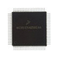
MC68HC912B32VFU8 Freescale Semiconductor, MC68HC912B32VFU8 Datasheet - Page 86

MC68HC912B32VFU8
Manufacturer Part Number
MC68HC912B32VFU8
Description
Manufacturer
Freescale Semiconductor
Datasheet
1.MC68HC912B32VFU8.pdf
(334 pages)
Specifications of MC68HC912B32VFU8
Cpu Family
HC12
Device Core Size
16b
Frequency (max)
8MHz
Interface Type
SCI/SPI
Program Memory Type
EPROM
Program Memory Size
32KB
Total Internal Ram Size
1KB
# I/os (max)
63
Operating Supply Voltage (typ)
5V
Operating Supply Voltage (max)
5.5V
Operating Supply Voltage (min)
4.5V
On-chip Adc
8-chx10-bit
Instruction Set Architecture
CISC
Operating Temp Range
-40C to 105C
Operating Temperature Classification
Industrial
Mounting
Surface Mount
Pin Count
80
Package Type
PQFP
Lead Free Status / Rohs Status
Not Compliant
Available stocks
Company
Part Number
Manufacturer
Quantity
Price
Part Number:
MC68HC912B32VFU8
Manufacturer:
MOTOROLA/摩托罗拉
Quantity:
20 000
- Current page: 86 of 334
- Download datasheet (2Mb)
Bus Control and Input/Output (I/O)
be set. In this special case of expanded mode and EME set, the port E data register (PORTE) and port E
data direction register (DDRE) are removed from the on-chip memory map and become external
accesses so port E may be rebuilt externally.
6.3.1 Port A Data Register
Read: Anytime, if register is in the map
Write: Anytime, if register is in the map
Bits PA7–PA0 are associated with addresses ADDR15–ADDR8 and DATA15–DATA8. When this port is
not used for external addresses and data, such as in single-chip mode, these pins can be used as
general-purpose input/output (I/O). DDRA determines the primary direction of each pin. This register is
not in the on-chip map in expanded and peripheral modes.
6.3.2 Port A Data Direction Register
Read: Anytime, if register is in the map
Write: Anytime, if register is in the map
This register determines the primary direction for each port A pin when functioning as a general-purpose
I/O port. DDRA is not in the on-chip map in expanded and peripheral modes.
86
Expanded wide and peripheral:
1 = Associated pin is an output.
0 = Associated pin is a high-impedance input.
Address: $0002
Expanded narrow:
Reset:
Read:
Write:
Address: $0000
Reset:
Read:
Write:
DDA7
Bit 7
0
Figure 6-2. Port A Data Direction Register (DDRA)
DATA15/7
ADDR15
ADDR15
DATA15
Bit 7
PA7
Figure 6-1. Port A Data Register (PORTA)
DDA6
6
0
M68HC12B Family Data Sheet, Rev. 9.1
DATA14/6
ADDR14
ADDR14
DATA14
PA6
6
DDA5
5
0
DATA13/5
ADDR13
ADDR13
DATA13
PA5
5
DDA4
4
0
DATA12/4
ADDR12
ADDR12
DATA12
Unaffected by reset
PA4
4
DDA3
3
0
DATA11/3
ADDR11
ADDR11
DATA11
PA3
DDA2
3
2
0
DATA10/2
ADDR10
ADDR10
DATA10
PA2
DDA1
2
1
0
DATA9/1
Freescale Semiconductor
ADDR9
ADDR9
DATA9
PA1
DDA0
1
Bit 0
0
DATA8/0
ADDR8
ADDR8
DATA8
Bit 0
PA0
Related parts for MC68HC912B32VFU8
Image
Part Number
Description
Manufacturer
Datasheet
Request
R
Part Number:
Description:
Manufacturer:
Freescale Semiconductor, Inc
Datasheet:
Part Number:
Description:
Manufacturer:
Freescale Semiconductor, Inc
Datasheet:
Part Number:
Description:
Manufacturer:
Freescale Semiconductor, Inc
Datasheet:
Part Number:
Description:
Manufacturer:
Freescale Semiconductor, Inc
Datasheet:
Part Number:
Description:
Manufacturer:
Freescale Semiconductor, Inc
Datasheet:
Part Number:
Description:
Manufacturer:
Freescale Semiconductor, Inc
Datasheet:
Part Number:
Description:
Manufacturer:
Freescale Semiconductor, Inc
Datasheet:
Part Number:
Description:
Manufacturer:
Freescale Semiconductor, Inc
Datasheet:
Part Number:
Description:
Manufacturer:
Freescale Semiconductor, Inc
Datasheet:
Part Number:
Description:
Manufacturer:
Freescale Semiconductor, Inc
Datasheet:
Part Number:
Description:
Manufacturer:
Freescale Semiconductor, Inc
Datasheet:
Part Number:
Description:
Manufacturer:
Freescale Semiconductor, Inc
Datasheet:
Part Number:
Description:
Manufacturer:
Freescale Semiconductor, Inc
Datasheet:
Part Number:
Description:
Manufacturer:
Freescale Semiconductor, Inc
Datasheet:
Part Number:
Description:
Manufacturer:
Freescale Semiconductor, Inc
Datasheet:


