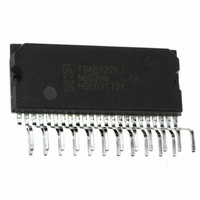
TDA8920CJ/N1,112 NXP Semiconductors, TDA8920CJ/N1,112 Datasheet - Page 11

TDA8920CJ/N1,112
Manufacturer Part Number
TDA8920CJ/N1,112
Description
IC AMP AUDIO PWR 220W 23SIL
Manufacturer
NXP Semiconductors
Type
Class Dr
Datasheet
1.TDA8920CJN1112.pdf
(39 pages)
Specifications of TDA8920CJ/N1,112
Output Type
1-Channel (Mono) or 2-Channel (Stereo)
Package / Case
23-SIL (Bent and Staggered Leads)
Max Output Power X Channels @ Load
220W x 1 @ 8 Ohm; 125W x 2 @ 4 Ohm
Voltage - Supply
±12.5 V ~ 32.5 V
Features
Depop, Differential Inputs, Mute, Short-Circuit and Thermal Protection, Standby
Mounting Type
Through Hole
Product
Class-D
Output Power
210 W
Available Set Gain
36 dB
Common Mode Rejection Ratio (min)
75 dB
Thd Plus Noise
0.05 %
Maximum Operating Temperature
+ 85 C
Mounting Style
Through Hole
Audio Load Resistance
8 Ohms
Dual Supply Voltage
+/- 30 V
Input Signal Type
Differential
Minimum Operating Temperature
- 40 C
Output Signal Type
Differential, Single
Supply Type
Dual
Lead Free Status / RoHS Status
Lead free / RoHS Compliant
Other names
568-4784-5
935281808112
TDA8920CJ/N1
TDA8920CJ/N1,112
TDA8920CJ/N1
935281808112
TDA8920CJ/N1
TDA8920CJ/N1,112
TDA8920CJ/N1
NXP Semiconductors
TDA8920C_2
Product data sheet
8.3.4 Supply voltage protection
8.4 Differential audio inputs
If the supply voltage drops below the minimum supply voltage threshold, V
circuit will be activated and the system will shut down. Once the supply voltage rises
above V
If the supply voltage exceeds the maximum supply voltage threshold, V
circuit will be activated and the power stages will be shut down. When the supply voltage
drops below V
An additional UnBalance Protection (UBP) circuit compares the positive analog supply
voltage (on pin VDDA) with the negative analog supply voltage (on pin VSSA) and is
triggered if the voltage difference exceeds a factor of two (V
2
V
An overview of all protection circuits and their respective effects on the output signal is
provided in
Table 5.
[1]
[2]
[3]
The audio inputs are fully differential ensuring a high common mode rejection ratio and
maximum flexibility in the application.
Protection name Complete
TFB
OTP
OCP
WP
UVP
OVP
UBP
P(ubp)
•
•
V
Amplifier gain depends on the junction temperature and heatsink size.
The amplifier shuts down completely only if the short-circuit impedance is below the impedance threshold
(Z
Fault condition detected during any Standby-to-Mute transition or during a restart after OCP has been
activated (short-circuit to one of the supply lines).
Stereo operation: to avoid acoustical phase differences, the inputs should be in
antiphase and the speakers should be connected in antiphase. This configuration:
– minimizes power supply peak current
– minimizes supply pumping effects, especially at low audio frequencies
Mono BTL operation: the inputs must be connected in anti-parallel. The output of one
channel is inverted and the speaker load is connected between the two outputs of the
TDA8920C. In practice (because of the OCP threshold) the output power can be
boosted to twice the output power that can be achieved with the single-ended
configuration.
The input configuration for a mono BTL application is illustrated in
[1]
DDA
th
, the system restarts after 100 ms.
; see
P(uvp)
). When the supply voltage difference drops below the unbalance threshold,
Overview of TDA8920C protection circuits
Section
Table
again, the system will restart after a delay of 100 ms.
P(ovp)
5.
8.3.2). In all other cases, current limiting results in a clipped output signal.
shutdown
N
Y
Y
N
Y
Y
Y
[2]
[3]
again, the system will restart after a delay of 100 ms.
Rev. 02 — 11 June 2009
Restart directly
N
N
N
Y
N
N
N
[2]
2
Restart after
100 ms
N
Y
Y
N
Y
Y
Y
[2]
110 W class-D power amplifier
DDA
> 2
TDA8920C
V
Figure
© NXP B.V. 2009. All rights reserved.
P(ovp)
SSA
Pin PROT
detection
N
N
Y
N
N
N
N
P(uvp)
OR V
, the OVP
7.
, the UVP
SSA
11 of 39
>


