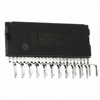
TDA8920CJ/N1,112 NXP Semiconductors, TDA8920CJ/N1,112 Datasheet - Page 14

TDA8920CJ/N1,112
Manufacturer Part Number
TDA8920CJ/N1,112
Description
IC AMP AUDIO PWR 220W 23SIL
Manufacturer
NXP Semiconductors
Type
Class Dr
Datasheet
1.TDA8920CJN1112.pdf
(39 pages)
Specifications of TDA8920CJ/N1,112
Output Type
1-Channel (Mono) or 2-Channel (Stereo)
Package / Case
23-SIL (Bent and Staggered Leads)
Max Output Power X Channels @ Load
220W x 1 @ 8 Ohm; 125W x 2 @ 4 Ohm
Voltage - Supply
±12.5 V ~ 32.5 V
Features
Depop, Differential Inputs, Mute, Short-Circuit and Thermal Protection, Standby
Mounting Type
Through Hole
Product
Class-D
Output Power
210 W
Available Set Gain
36 dB
Common Mode Rejection Ratio (min)
75 dB
Thd Plus Noise
0.05 %
Maximum Operating Temperature
+ 85 C
Mounting Style
Through Hole
Audio Load Resistance
8 Ohms
Dual Supply Voltage
+/- 30 V
Input Signal Type
Differential
Minimum Operating Temperature
- 40 C
Output Signal Type
Differential, Single
Supply Type
Dual
Lead Free Status / RoHS Status
Lead free / RoHS Compliant
Other names
568-4784-5
935281808112
TDA8920CJ/N1
TDA8920CJ/N1,112
TDA8920CJ/N1
935281808112
TDA8920CJ/N1
TDA8920CJ/N1,112
TDA8920CJ/N1
NXP Semiconductors
12. Dynamic characteristics
Table 9.
V
[1]
[2]
[3]
TDA8920C_2
Product data sheet
Symbol
Internal oscillator
f
f
External oscillator input or frequency tracking; pin OSC
V
V
f
Z
C
t
osc(typ)
osc
track
r(i)
P
OSC
trip
i
i
[1]
V
When using an external oscillator, the frequency f
(250 kHz minimum, 450 kHz maximum) due to the internal clock divider; see
When t
= 30 V; T
P
is the supply voltage on pins VDDP1, VDDP2 and VDDA.
r(i)
Dynamic characteristics
> 100 ns, the output noise floor will increase.
Parameter
typical oscillator frequency R
oscillator frequency
voltage on pin OSC
trip voltage
tracking frequency
input impedance
input capacitance
input rise time
amb
12.1 Switching characteristics
= 25 C; unless otherwise specified.
Fig 8.
V
Behavior of mode selection pin MODE
O(offset)(mute)
V
O(offset)(on)
V
O
Conditions
HIGH-level
from SGND + 0 V to
SGND + 5 V
(V)
OSC
= 30.0 k
0
track
Standby
Rev. 02 — 11 June 2009
(500 kHz minimum, 900 kHz maximum) will result in a PWM frequency f
0.8
[3]
[2]
slope is directly related to the time-constant
Min
290
250
SGND + 4.5
-
500
1
-
-
of the RC network on the MODE pin
2.2
Section
Mute
8.2.
3.0
2
Typ
345
-
SGND + 5
SGND + 2.5
-
-
-
-
110 W class-D power amplifier
4.2
V
MODE
TDA8920C
On
Max
365
450
SGND + 6
-
900
-
15
100
© NXP B.V. 2009. All rights reserved.
(V)
5.5
coa021
osc
14 of 39
Unit
kHz
kHz
V
V
kHz
M
pF
ns


