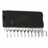
TDA8920CJ/N1,112 NXP Semiconductors, TDA8920CJ/N1,112 Datasheet - Page 35

TDA8920CJ/N1,112
Manufacturer Part Number
TDA8920CJ/N1,112
Description
IC AMP AUDIO PWR 220W 23SIL
Manufacturer
NXP Semiconductors
Type
Class Dr
Datasheet
1.TDA8920CJN1112.pdf
(39 pages)
Specifications of TDA8920CJ/N1,112
Output Type
1-Channel (Mono) or 2-Channel (Stereo)
Package / Case
23-SIL (Bent and Staggered Leads)
Max Output Power X Channels @ Load
220W x 1 @ 8 Ohm; 125W x 2 @ 4 Ohm
Voltage - Supply
±12.5 V ~ 32.5 V
Features
Depop, Differential Inputs, Mute, Short-Circuit and Thermal Protection, Standby
Mounting Type
Through Hole
Product
Class-D
Output Power
210 W
Available Set Gain
36 dB
Common Mode Rejection Ratio (min)
75 dB
Thd Plus Noise
0.05 %
Maximum Operating Temperature
+ 85 C
Mounting Style
Through Hole
Audio Load Resistance
8 Ohms
Dual Supply Voltage
+/- 30 V
Input Signal Type
Differential
Minimum Operating Temperature
- 40 C
Output Signal Type
Differential, Single
Supply Type
Dual
Lead Free Status / RoHS Status
Lead free / RoHS Compliant
Other names
568-4784-5
935281808112
TDA8920CJ/N1
TDA8920CJ/N1,112
TDA8920CJ/N1
935281808112
TDA8920CJ/N1
TDA8920CJ/N1,112
TDA8920CJ/N1
NXP Semiconductors
TDA8920C_2
Product data sheet
15.4 Reflow soldering
Key characteristics in reflow soldering are:
Table 12.
Table 13.
Moisture sensitivity precautions, as indicated on the packing, must be respected at all
times.
Studies have shown that small packages reach higher temperatures during reflow
soldering, see
Package thickness (mm)
< 2.5
Package thickness (mm)
< 1.6
1.6 to 2.5
> 2.5
•
•
•
2.5
Lead-free versus SnPb soldering; note that a lead-free reflow process usually leads to
higher minimum peak temperatures (see
reducing the process window
Solder paste printing issues including smearing, release, and adjusting the process
window for a mix of large and small components on one board
Reflow temperature profile; this profile includes preheat, reflow (in which the board is
heated to the peak temperature) and cooling down. It is imperative that the peak
temperature is high enough for the solder to make reliable solder joints (a solder paste
characteristic). In addition, the peak temperature must be low enough that the
packages and/or boards are not damaged. The peak temperature of the package
depends on package thickness and volume and is classified in accordance with
Table 12
SnPb eutectic process (from J-STD-020C)
Lead-free process (from J-STD-020C)
and
Figure
13
30.
Rev. 02 — 11 June 2009
Package reflow temperature ( C)
Volume (mm
< 350
235
220
Package reflow temperature ( C)
Volume (mm
< 350
260
260
250
3
3
)
)
Figure
350 to 2000
260
250
245
30) than a SnPb process, thus
2
110 W class-D power amplifier
220
220
350
TDA8920C
> 2000
260
245
245
© NXP B.V. 2009. All rights reserved.
35 of 39


