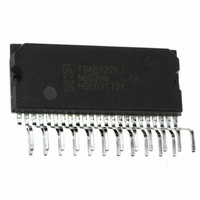
TDA8920CJ/N1,112 NXP Semiconductors, TDA8920CJ/N1,112 Datasheet - Page 12

TDA8920CJ/N1,112
Manufacturer Part Number
TDA8920CJ/N1,112
Description
IC AMP AUDIO PWR 220W 23SIL
Manufacturer
NXP Semiconductors
Type
Class Dr
Datasheet
1.TDA8920CJN1112.pdf
(39 pages)
Specifications of TDA8920CJ/N1,112
Output Type
1-Channel (Mono) or 2-Channel (Stereo)
Package / Case
23-SIL (Bent and Staggered Leads)
Max Output Power X Channels @ Load
220W x 1 @ 8 Ohm; 125W x 2 @ 4 Ohm
Voltage - Supply
±12.5 V ~ 32.5 V
Features
Depop, Differential Inputs, Mute, Short-Circuit and Thermal Protection, Standby
Mounting Type
Through Hole
Product
Class-D
Output Power
210 W
Available Set Gain
36 dB
Common Mode Rejection Ratio (min)
75 dB
Thd Plus Noise
0.05 %
Maximum Operating Temperature
+ 85 C
Mounting Style
Through Hole
Audio Load Resistance
8 Ohms
Dual Supply Voltage
+/- 30 V
Input Signal Type
Differential
Minimum Operating Temperature
- 40 C
Output Signal Type
Differential, Single
Supply Type
Dual
Lead Free Status / RoHS Status
Lead free / RoHS Compliant
Other names
568-4784-5
935281808112
TDA8920CJ/N1
TDA8920CJ/N1,112
TDA8920CJ/N1
935281808112
TDA8920CJ/N1
TDA8920CJ/N1,112
TDA8920CJ/N1
NXP Semiconductors
9. Limiting values
Table 6.
In accordance with the Absolute Maximum Rating System (IEC 60134).
[1]
10. Thermal characteristics
TDA8920C_2
Product data sheet
Symbol
V
I
T
T
T
V
V
V
V
V
I
V
ORM
q(tot)
P
stg
amb
j
MODE
OSC
I
PROT
ESD
PWM(p-p)
[1]
V
P
is the supply voltage on pins VDDP1, VDDP2 and VDDA.
Limiting values
Parameter
supply voltage
repetitive peak output current
storage temperature
ambient temperature
junction temperature
voltage on pin MODE
voltage on pin OSC
input voltage
voltage on pin PROT
electrostatic discharge voltage
total quiescent current
peak-to-peak PWM voltage
Table 7.
Symbol
R
R
Fig 7.
th(j-a)
th(j-c)
Input configuration for mono BTL application
Thermal characteristics
Parameter
thermal resistance from junction to ambient
thermal resistance from junction to case
V
in
Conditions
Standby, Mute modes; V
maximum output current limiting
referenced to SGND
referenced to SGND; pin IN1P; IN1M;
IN2P and IN2M
referenced to voltage on pin VSSD
Human Body Model (HBM)
Charged Device Model (CDM)
Operating mode; no load; no filter; no
RC-snubber network connected
on pins OUT1 and OUT2
Rev. 02 — 11 June 2009
IN1M
IN2M
IN1P
IN2P
power stage
DD
V
SS
2
OUT1
OUT2
Conditions
in free air
mbl466
110 W class-D power amplifier
SGND
Min
-
9.2
-
0
0
0
-
-
55
40
5
2000
500
TDA8920C
© NXP B.V. 2009. All rights reserved.
Max
65
-
+150
+85
150
6
SGND + 6
+5
12
+2000
+500
75
120
Typ
40
1.1
Unit
K/W
K/W
12 of 39
Unit
V
A
V
V
V
V
V
V
mA
V
C
C
C


