BLF6G15LS-40RN NXP Semiconductors, BLF6G15LS-40RN Datasheet
BLF6G15LS-40RN


Related parts for BLF6G15LS-40RN


BLF6G15LS-40RN Summary of contents
Page 1
... BLF6G15L-40RN; BLF6G15LS-40RN Power LDMOS transistor Rev. 1 — 27 October 2011 1. Product profile 1.1 General description 40 W LDMOS power transistor for base station applications at frequencies from 1450 MHz to 1550 MHz. Table 1. Typical RF performance at T Test signal 2-carrier W-CDMA [1] Test signal: 3GPP test model 1; 64 DPCH; PAR = 7 probability of 0. CCDF carrier; ...
Page 2
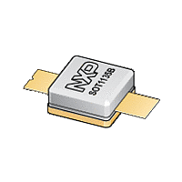
... NXP Semiconductors 2. Pinning information Table 2. Pin BLF6G15L-40RN (SOT1135A BLF6G15LS-40RN (SOT1135B [1] Connected to flange. 3. Ordering information Table 3. Type number BLF6G15L-40RN BLF6G15LS-40RN 4. Limiting values Table 4. In accordance with the Absolute Maximum Rating System (IEC 60134). Symbol stg T j BLF6G15L-40RN_6G15LS-40RN ...
Page 3
... NXP Semiconductors 5. Thermal characteristics Table 5. Symbol Parameter R th(j-case) 6. Characteristics Table 6. Symbol Parameter V (BR)DSS V GS(th) I DSS I DSX I GSS DS(on) 7. Application information Table 7. Class-AB production test circuit; PAR 7 0.01 % probability on CCDF; 3GPP test model 1; 64 DPCH Symbol ...
Page 4
... NXP Semiconductors 8. Package outline Flanged ceramic package; 2 mounting holes; 2 leads Dimensions (1) Unit max 4.65 5.26 0.18 9.65 mm nom min 3.76 5.00 0.10 9.40 max 0.183 0.207 0.007 0.38 inches nom min 0.148 0.197 0.004 0.37 Note 1. millimeter dimensions are derived from the original inch dimensions. 2. dimension is measured 0.030 inch (0.76 mm) from the body. ...
Page 5
... NXP Semiconductors Earless flanged ceramic package; 2 leads Dimensions (1) Unit max 4.65 5.26 0.18 9.65 mm nom min 3.76 5.00 0.10 9.40 max 0.183 0.207 0.007 0.38 inches nom min 0.148 0.197 0.004 0.37 Note 1. millimeter dimensions are derived from the original inch dimensions. 2. dimension is measured 0.030 inch (0.76 mm) from the body. ...
Page 6
... NXP Semiconductors 9. Handling information CAUTION This device is sensitive to ElectroStatic Discharge (ESD). Observe precautions for handling electrostatic sensitive devices. Such precautions are described in the ANSI/ESD S20.20, IEC/ST 61340-5, JESD625-A or equivalent standards. 10. Abbreviations Table 8. Acronym 3GPP CCDF CW LDMOS PAR DPCH RF VSWR W-CDMA 11. Revision history Table 9 ...
Page 7
... In no event shall NXP Semiconductors be liable for any indirect, incidental, punitive, special or consequential damages (including - without limitation - lost profits, lost savings, business interruption, costs related to the removal or ...
Page 8
... Objective data sheet NXP Semiconductors’ specifications such use shall be solely at customer’s own risk, and (c) customer fully indemnifies NXP Semiconductors for any liability, damages or failed product claims resulting from customer design and use of the product for automotive applications beyond NXP Semiconductors’ ...
Page 9
... NXP Semiconductors 14. Contents 1 Product profile . . . . . . . . . . . . . . . . . . . . . . . . . . 1 1.1 General description . . . . . . . . . . . . . . . . . . . . . 1 1.2 Features and benefits . . . . . . . . . . . . . . . . . . . . 1 1.3 Applications . . . . . . . . . . . . . . . . . . . . . . . . . . . 1 2 Pinning information . . . . . . . . . . . . . . . . . . . . . . 2 3 Ordering information . . . . . . . . . . . . . . . . . . . . . 2 4 Limiting values Thermal characteristics . . . . . . . . . . . . . . . . . . 3 6 Characteristics . . . . . . . . . . . . . . . . . . . . . . . . . . 3 7 Application information Package outline . . . . . . . . . . . . . . . . . . . . . . . . . 4 9 Handling information Abbreviations . . . . . . . . . . . . . . . . . . . . . . . . . . . 6 11 Revision history . . . . . . . . . . . . . . . . . . . . . . . . . 6 12 Legal information ...