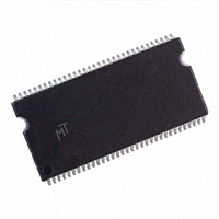
MT46V8M16TG-6T L:D TR Micron Technology Inc, MT46V8M16TG-6T L:D TR Datasheet - Page 13

MT46V8M16TG-6T L:D TR
Manufacturer Part Number
MT46V8M16TG-6T L:D TR
Description
IC DDR SDRAM 128MBIT 6NS 66TSOP
Manufacturer
Micron Technology Inc
Datasheet
1.MT46V16M8TG-6T_LD_TR.pdf
(81 pages)
Specifications of MT46V8M16TG-6T L:D TR
Format - Memory
RAM
Memory Type
DDR SDRAM
Memory Size
128M (8Mx16)
Speed
6ns
Interface
Parallel
Voltage - Supply
2.3 V ~ 2.7 V
Operating Temperature
0°C ~ 70°C
Package / Case
66-TSOP
Lead Free Status / RoHS Status
Contains lead / RoHS non-compliant
Other names
557-1042-2
Table 7:
PDF: 09005aef816fd013/Source: 09005aef82a95a3a
128Mb_DDR_x4x8x16_D2.fm - 128Mb DDR: Rev. F; Core DDR: Rev. A 4/07 EN
Parameter/Condition
Operating one-bank active-precharge current:
t
changing once per clock cycle; Address and control inputs
changing once every two clock cycles
Operating one-bank active-read-precharge current:
Burst = 2;
Address and control inputs
Precharge power-down standby current: All banks idle;
Power-down mode;
Idle standby current: CS# = HIGH; All banks are idle;
t
changing once per clock
Active power-down standby current: One bank active;
down mode;
Active standby current: CS# = HIGH; CKE = HIGH; One bank
active
inputs changing twice per clock cycle; Address and other control
inputs changing once per clock cycle
Operating burst read current: Burst = 2;
reads; One bank active; Address and control inputs changing once
per clock cycle;
Operating burst write current: Burst = 2; Continuous burst
writes;
once per clock cycle;
changing twice per clock cycle
Auto refresh burst current:
Self refresh current: CKE ≤ 0.2V
Operating bank interleave read current: Four bank
interleaving READs (Burst = 4) with auto precharge;
t
inputs change only during ACTIVE, READ, or WRITE commands
RC =
CK =
RC = minimum
;
t
t
RC (MIN);
CK (MIN);
t
One bank
RC =
t
RC =
t
I
V
0°C ≤ T
RAS (MAX);
t
DD
CK =
DD
t
t
CK =
RC allowed;
t
t
RC (MIN);
Q = +2.6V ±0.1V, V
CKE = HIGH; Address and other control inputs
Specifications and Conditions (x16; -5B, -6T, -75E -75Z -75)
CK =
active; Address and control inputs changing
t
t
A
CK (MIN); CKE = LOW
CK =
t
t
CK =
CK (MIN);
≤ +70°C; Notes: 1–5, 11, 13, 15, 47; Notes appear on pages 26–31; See also Table 8 on page 14
t
CK (MIN); DQ, DM, and DQS inputs
cycle.
t
t
CK =
CK (MIN); CKE = (LOW)
t
CK (MIN); DQ, DM, and DQS inputs
t
CK =
t
changing once per clock cycle
CK =
V
t
I
CK (MIN); DQ, DM, and DQS
IN
OUT
t
t
=
CK (MIN); I
CK (MIN); Address and control
DD
V
= 0mA
REF
= +2.6V ±0.1V (-5B); V
for DQ, DQS, and DM
Continuous burst
OUT
t
t
Standard
Low power (L)
RFC =
RFC = 15.6µs
= 0mA;
t
RFC (MIN)
Power-
13
DD
Q = +2.5V ±0.2V, V
Symbol -5B
I
I
I
I
I
I
I
I
DD
DD
DD
DD
DD
I
I
DD
DD
I
I
I
DD 2
Micron Technology, Inc., reserves the right to change products or specifications without notice.
DD
DD
DD
DD
DD
4W
3N
5A
6A
4R
2F
3P
0
1
5
6
7
P
125 125
135 135
185 165
185 165
265 265
385 385
1.3
50
30
50
10
128Mb: x4, x8, x16 DDR SDRAM
3
4
Electrical Specifications – I
DD
-6T
1.3
45
25
50
3
5
4
= +2.5V ±0.2V (-6T, -75E, -75Z, -75);
-75E -75Z/-75 Units
115
135
140
140
250
375
1.3
45
25
50
3
5
4
©2004 Micron Technology, Inc. All rights reserved.
110
125
140
140
250
375
1.3
40
25
45
3
5
4
mA
mA
mA
mA
mA
mA
mA
mA
mA
mA
mA
mA
mA
Notes
23, 48
23, 48
24, 33
24, 33
23, 48
28, 50
23, 49
51
23
23
50
12
12
DD


